Sputtering device

A sputtering equipment and sputtering technology, used in sputtering coating, ion implantation coating, metal material coating process, etc., can solve the problem of uneven thickness of ITO film

Inactive Publication Date: 2003-11-12
NIPPON SHEET GLASS CO LTD
View PDF4 Cites 12 Cited by
  • Summary
  • Abstract
  • Description
  • Claims
  • Application Information

AI Technical Summary

Problems solved by technology

[0018] Moreover, at the position corresponding to the power supply device 208 supported by the cathode case 209, the thickness of the

Method used


Image

  • Sputtering device
  • Sputtering device
  • Sputtering device

Examples


no. 1 example

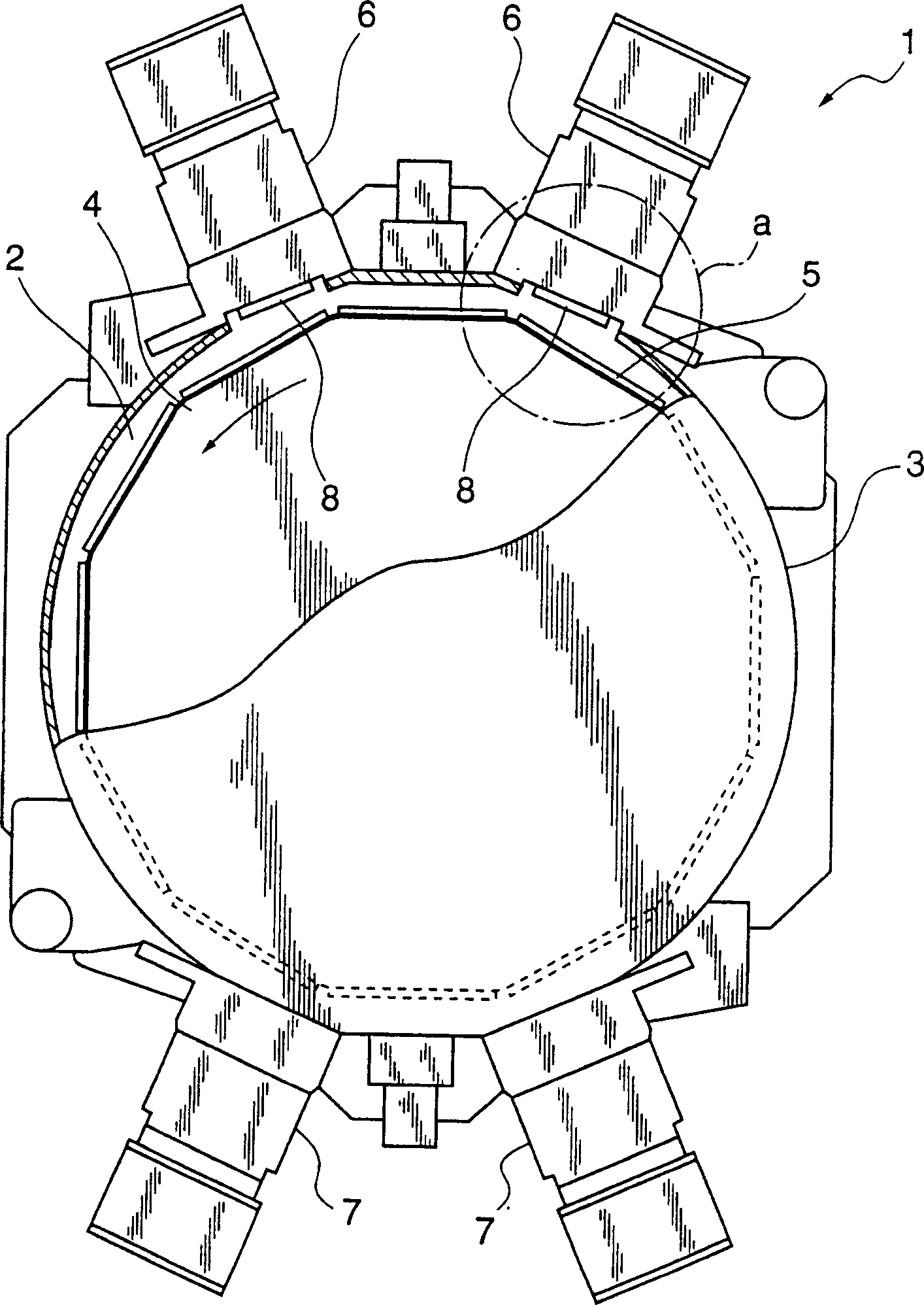
[0065] figure 1 is a partially cutaway plan view of a main body portion of a sputtering apparatus according to a first embodiment of the present invention.

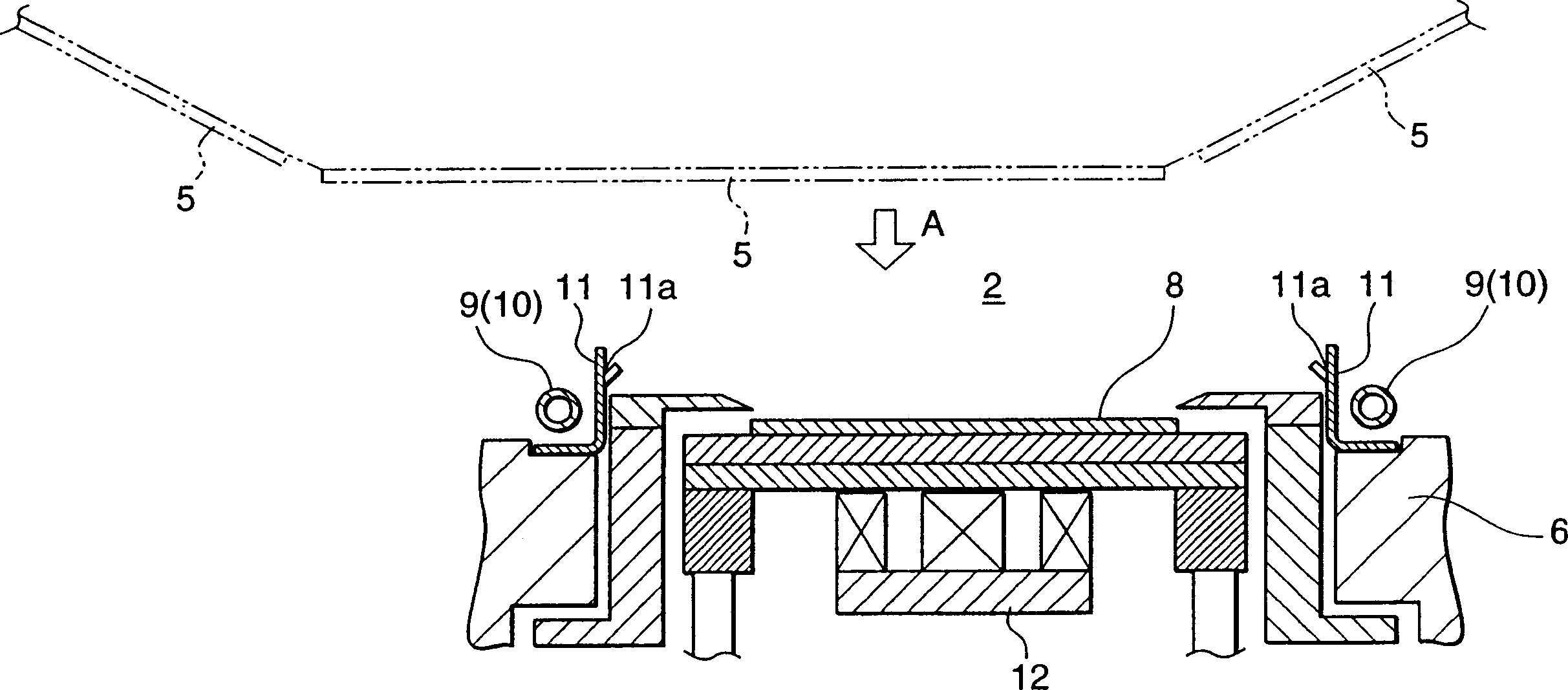
[0066] exist figure 1 Among them, the sputtering device 1 includes a housing 3 that forms a vacuum chamber 2 inside, and is located in the center of the housing 3 through a motor (not shown) along the figure 1 The dodecagonal rotating disc (substrate holder) 4 that rotates in the direction indicated by the arrow, a pair of ITO cathodes 6 that are used as sputtering cathodes at the peripheral side of the housing 3, and a pair of ITO cathodes that are connected to the ITO cathodes 6 Relative SiO 2 Cathode 7.

[0067] A plurality of substrates 5, for example four substrates 5, are arranged in a row on each side of the rotary disk 4 in the vertical direction. Each substrate 5 is a rectangular color filter substrate with a vertical dimension of 300 to 500 mm and a horizontal dimension of 400 to 600 mm, wherein a color f...

no. 2 example

[0130] Figure 11 is a partially cutaway plan view of a main body portion of a sputtering apparatus according to a second embodiment of the present invention.

[0131] exist Figure 11 Among them, the sputtering equipment 100 is formed by a housing 102 of a vacuum chamber 101 inside, and is located in the center of the housing 102 through a motor (moving device) (not shown) along the Figure 11 12 prismatic rotating discs (substrate holder) 103 that rotate in the direction shown by the arrow, a pair of ITO cathodes 104a and 104b that are used as sputtering cathodes at the peripheral side portion of the housing 102, and a pair of ITO cathodes with ITO Cathode 104a and 104b opposite SiO 2 Cathode 105a and 105b.

[0132] A plurality of substrates 106, for example four substrates 106, are arranged in a row on each side of the rotating disk 103 in the vertical direction. Each substrate 106 is a rectangular color filter substrate with a vertical dimension of 300 to 500 mm and a ...


PUM

PropertyMeasurementUnit
Resistivityaaaaaaaaaa
Thicknessaaaaaaaaaa

Abstract

A sputtering apparatus 1 sputters a target 8 with ions in a plasma using a magnetron sputtering method, to form an ITO film from the target 8 on glass substrates 5 mounted on a rotating carousel 4. Manifolds 9 and 10, which have a shape that is symmetrical about each of two mutually orthogonal central axes in the plane of the target 8, are disposed so as to surround the whole periphery of the target 8, and process gas discharge ports 9a and 10a for discharging a process gas onto the target 8 are provided in a manner being distributed over the whole of the manifolds 9 and 10.

Description

technical field [0001] The invention relates to a sputtering device, in particular to a sputtering device for manufacturing a substrate with a transparent conductive thin film used in a liquid crystal display device. Background technique [0002] A substrate with a transparent conductive film for a color liquid crystal display device is usually formed by coating a color filter layer made of an organic resin (organic substance) on a glass substrate, and then coating the color filter layer also made of an organic resin protective film to form a color filter substrate, and then uniformly form a transparent conductive electrode (transparent conductive film) on the color filter substrate. In this way, the transparent conductive film formed on the color filter substrate usually forms the required wiring structure by wet etching. Generally, indium oxide doped with tin oxide (hereinafter referred to as "indium oxide-tin (ITO)") is used as a material for forming the transparent cond...

Claims


Application Information

Patent Timeline
IPC IPC(8): C23C14/00C23C14/08
CPCC23C14/086C23C14/0063C23C14/34
Inventor 迫博明
Owner NIPPON SHEET GLASS CO LTD
Why Eureka
Try Eureka