

Method for producing bonded wafer
a technology of bonded wafers and oxide films, which is applied in the direction of semiconductor/solid-state device manufacturing, basic electric elements, electric apparatus, etc., can solve the problems of difficult to accommodate the further densification of mos-type devices in a current trend, difficult to achieve oxygen deposition in the monocrystal ingot of silicon, and deterioration of the resistance properties of gate oxide films, etc., to achieve the effect of increasing the throughput, reducing the cost of production
- Summary
- Abstract
- Description
- Claims
- Application Information
AI Technical Summary
Benefits of technology
Problems solved by technology
Method used
Image

Examples
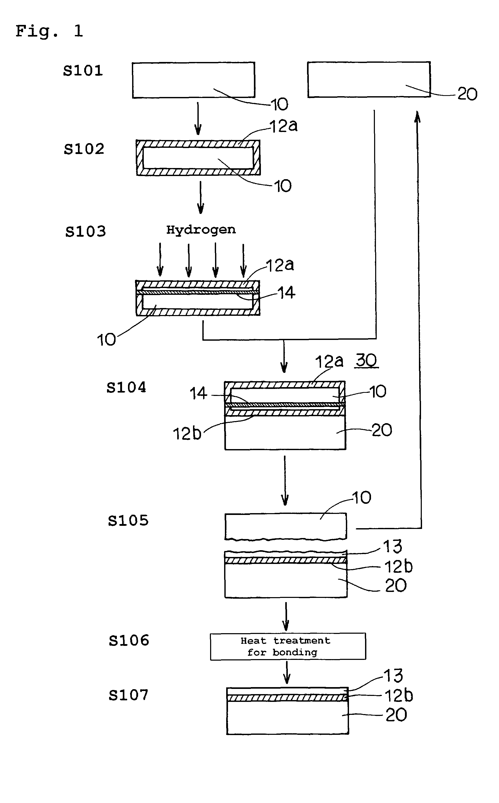
first embodiment
[0078]Firstly, a monocrystal ingot of silicon of p-type that has been doped with boron at a concentration as high as 1×10¹⁹ atmos / cm3 is pulled up in the CZ method as shown in step S101 of FIG. 1. A rate of pulling-up is 1.0 mm / min. A concentration of interstitial oxygen atom, Oi, of the monocrystal ingot of silicon is in a range of 11×1017 atoms / cm3 to 12×1017 atoms / cm3. After that, the monocrystal ingot of silicon undergoes a series of processing comprising block cutting, slicing, beveling and mirror polishing. Those steps of processing produce a wafer to be prepared as an active layer wafer 10 of p-type and mirror-polished having a thickness of 725 μm, a diameter of 200 mm and a specific resistance of 9 mΩcm.
[0079]On the other hand, a monocrystal ingot of silicon of p-type that has been added with the boron at a low concentration of 1×10¹⁵ atoms / cm3 is pulled up in the Cz method. After that, the monocrystal ingot of silicon undergoes a series of processing comprising block cuttin...
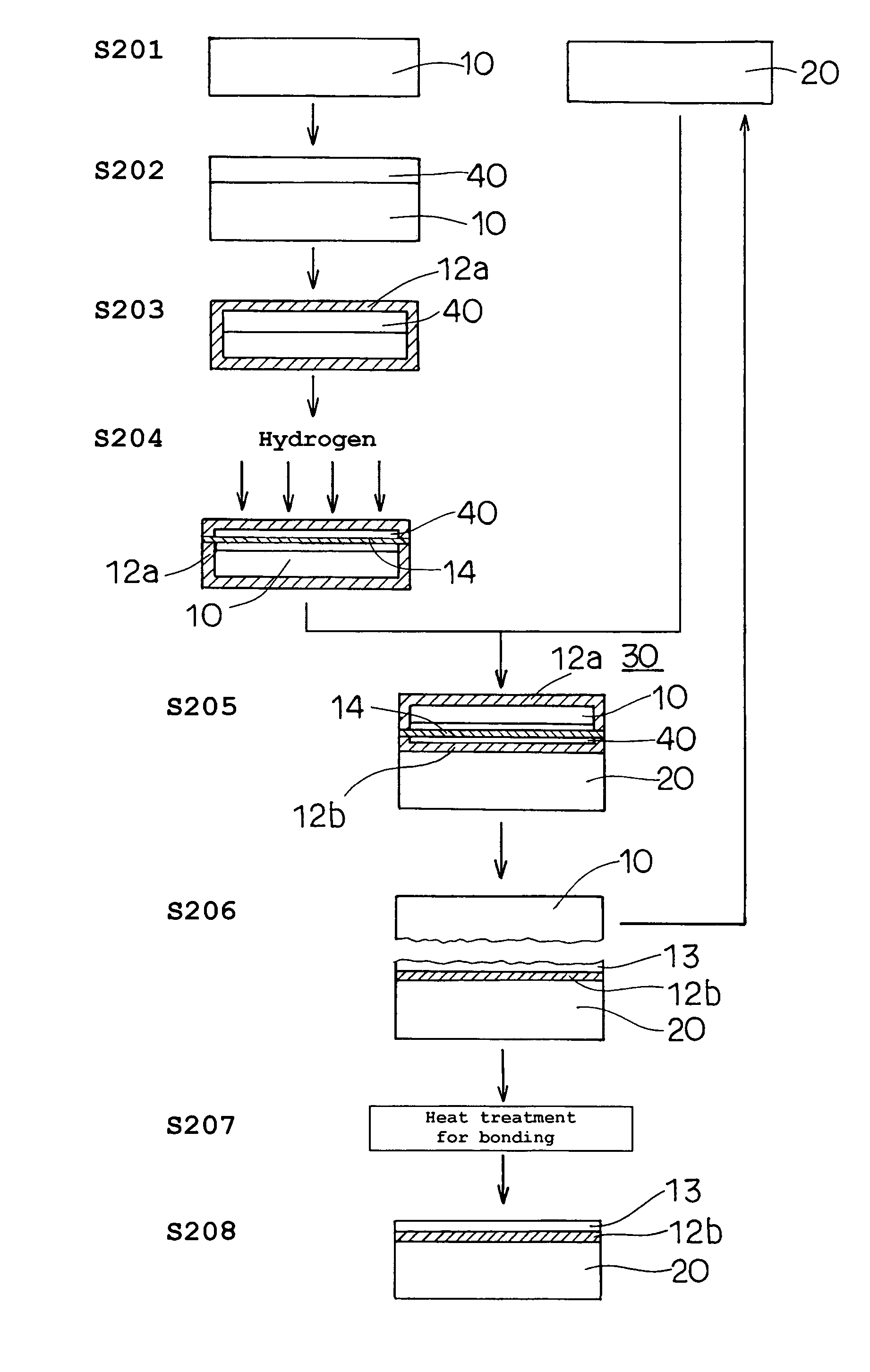
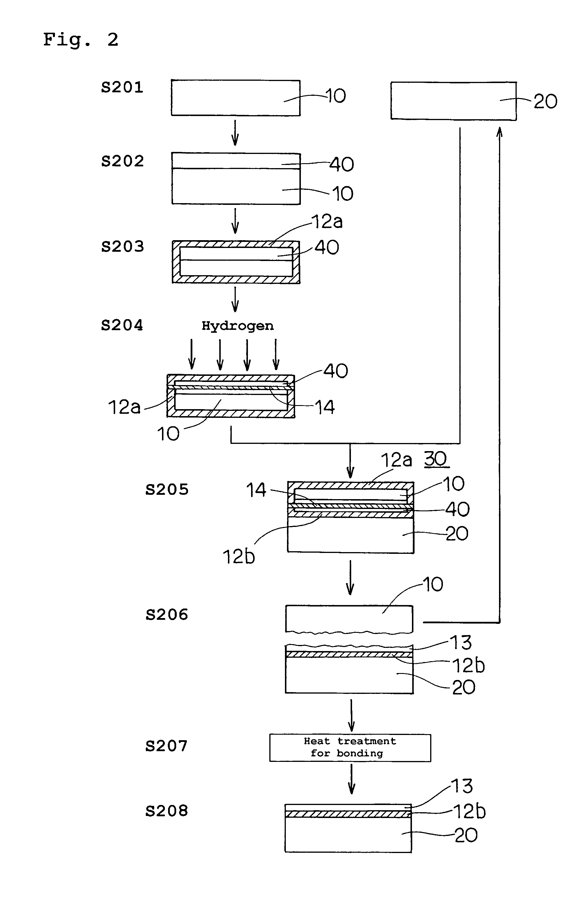
second embodiment
[0092]Turning now to FIG. 2, a method for producing a bonded wafer of a second embodiment will now be described. The second embodiment is characterized in that it is an example that has employed, instead of the active layer wafer 10 with the boron concentration of 1×10¹⁹atoms / cm3, an active layer wafer 10B comprising a main body containing the boron at a low concentration across the entire bulk thereof and an epitaxial layer 40 consisting of monocrystal silicon containing boron at a high concentration, which grows on the top surface of the main body.
[0093]The method for producing the bonded wafer of the second embodiment will be described more specifically below.
[0094]Firstly, a monocrystal ingot of silicon of p-type added with boron at a concentration as low as 1×10¹⁵ atmos / cm3 is pulled up in the CZ method as shown in step S201 of FIG. 2. A rate of pulling-up is 1.0 mm / min. After that, the monocrystal ingot of silicon undergoes a series of processing comprising block cutting, slic...
PUM
 Abstract
Description
Claims
Application Information