
Eureka
For R&D, Eureka makes reading and utilizing patents & technical documents easy.
Eureka AIR
Designed for self-driven R&D workflows. Generate viable solutions, solve complex R&D challenges, empower your innovation with AI.

Eureka Materials
Designed for material experts only. Revolutionize your material R&D, from search, analyze, to developing new materials.

TechResearch
Generate reliable direction feasibility study reports for your R&D in just a few steps.

TechSeek
Discover and master advanced knowledge NOW. Basics, ideas, possibilities, all at once.

TechMind
As an expert in R&D Theories, TechMind can generates customized viable solutions instantly.

TechRisk
Analyze your overall solution with one click, know your potential R&D risks in advance.

TechMonitor
Get weekly tech updates, stay abreast of the latest tech innovations and key insights.
Flash electric charge amplification structure focal plane reading-out circuit and its reset reading-out method
A charge amplification and readout circuit technology, applied in TV, electrical components, color TV, etc., can solve the problems of excessive transient peak current, limited area, and reduce the signal-to-noise ratio of the circuit, so as to reduce the transient peak current , Large charge storage capacity, the effect of reducing FPN noise
- Summary
- Abstract
- Description
- Claims
- Application Information
AI Technical Summary
Problems solved by technology
Method used
Image

Examples
Embodiment Construction
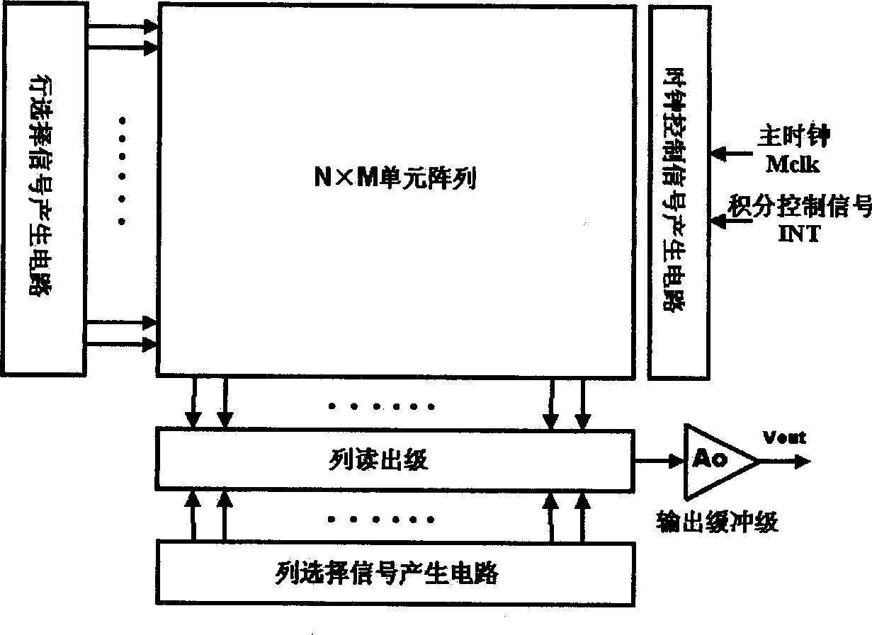
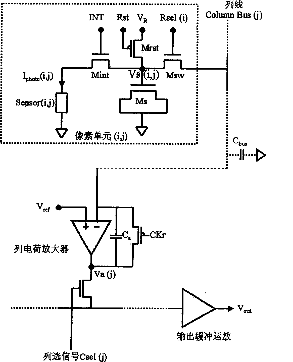
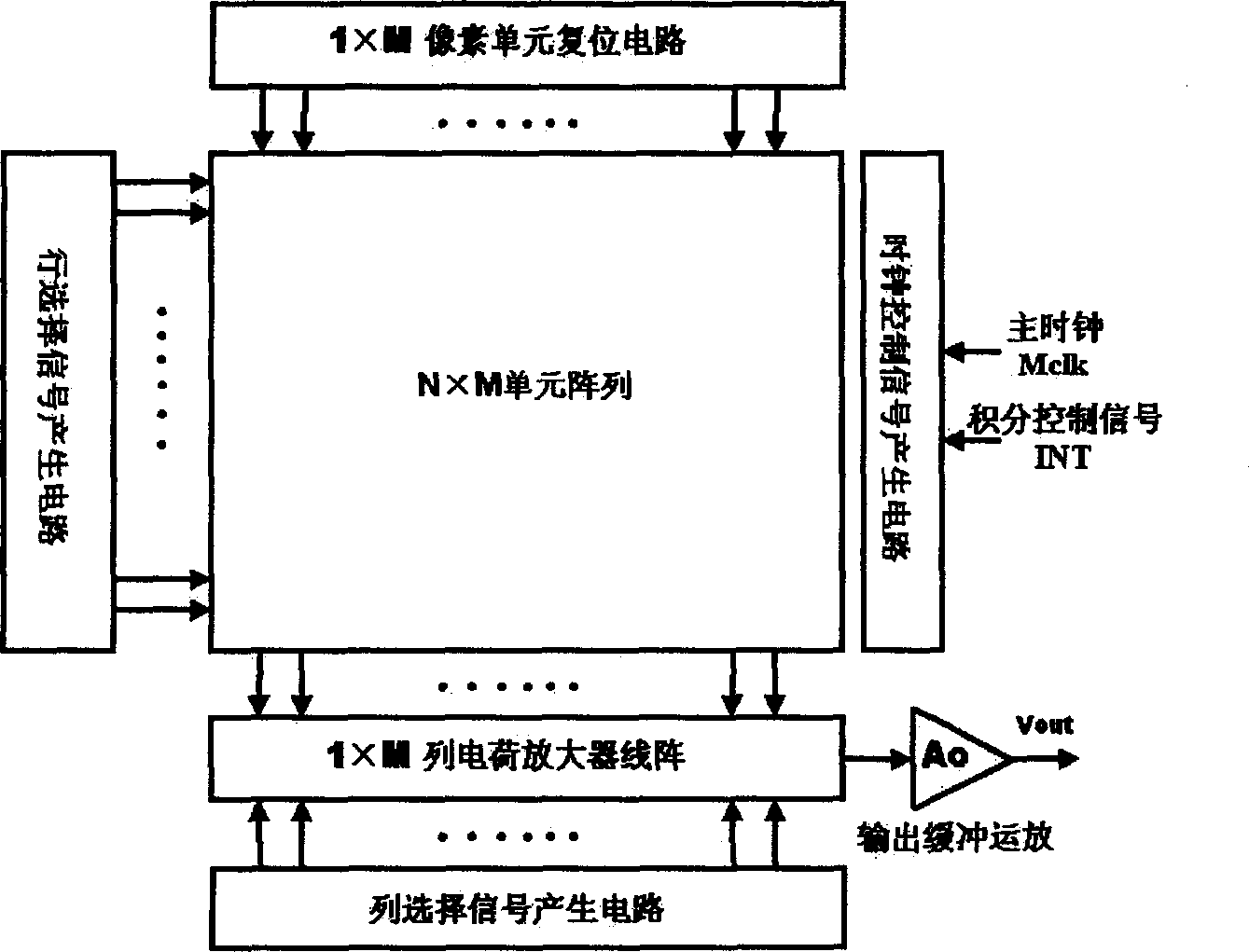
[0056] The focal plane readout circuit with a flash charge amplification structure using a row-by-row reset structure, the overall block diagram is as follows image 3 As shown, its unit circuit and architecture are as follows Figure 4 shown. The standard CMOS process is adopted, and the array scale is N×M. In this embodiment, N=M=130.
[0057] refer to image 3 with Figure 4 As shown, the whole circuit includes the following parts:
[0058] 1. An N×M-scale unit circuit array receives optical signals and completes the conversion and integration of photoelectric signals; each pixel unit consists of two switch tubes (Mint and Msw) and a transistor (Ms) used as a MOS capacitor.
[0059] 2. The 1×N scale shift register array is used to generate the row selection signal Rsel(i). Under the control of the row selection signal Rsel(i), the signal (charge) in the pixel unit is transferred to the column readout stage row by row ;
[0060] 3. The 1×M scale shift register array i...
PUM
 Abstract
Description
Claims
Application Information
 - R&D Engineer
- R&D Manager
- IP Professional
- Industry Leading Data Capabilities
- Powerful AI technology
- Patent DNA Extraction
Browse by: Latest US Patents, China's latest patents, Technical Efficacy Thesaurus, Application Domain, Technology Topic, Popular Technical Reports.
© 2024 PatSnap. All rights reserved.Legal|Privacy policy|Modern Slavery Act Transparency Statement|Sitemap|About US| Contact US: help@patsnap.com