Manufacturing method of semiconductor assembly part capable of improving lattice defectin silicon build up crystal layer

A manufacturing method and technology of lattice defects, applied in semiconductor/solid-state device manufacturing, electrical components, circuits, etc., can solve problems such as lattice defects, leakage current of shallow junction components, and reliability of component characteristics

Inactive Publication Date: 2004-03-03
GRACE SEMICON MFG CORP
View PDF0 Cites 7 Cited by
  • Summary
  • Abstract
  • Description
  • Claims
  • Application Information

AI Technical Summary

Problems solved by technology

[0005] However, in the steps of the above-mentioned known semiconductor manufacturing method, when growing a silicon epitaxial layer 20 on the source / drain 22 to form a raised source / drain structure, it is very easy to have crystals in the silicon epitaxial layer 20. The generation of crystal defects; and the defects generated in the crystal lattice of the silicon epitaxial layer 20 will cause leakage current (leakage current) phenomenon in the shallow junction components, thereby affecting the characteristics and reliability of the components

Method used


Image

  • Manufacturing method of semiconductor assembly part capable of improving lattice defectin silicon build up crystal layer
  • Manufacturing method of semiconductor assembly part capable of improving lattice defectin silicon build up crystal layer
  • Manufacturing method of semiconductor assembly part capable of improving lattice defectin silicon build up crystal layer

Examples


Embodiment Construction

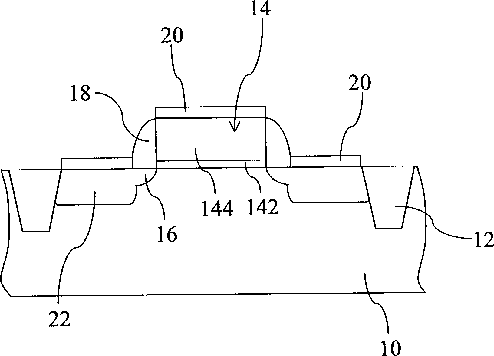
[0016] When the known technology grows a silicon epitaxial layer on the source / drain to form a raised source / drain structure, it is very easy to have lattice defects in the silicon epitaxial layer; and the semiconductor proposed by the present invention The component manufacturing method can solve the crystal lattice defects in the silicon epitaxy layer, so as to avoid the leakage current phenomenon of the silicon epitaxy layer at the shallow junction.

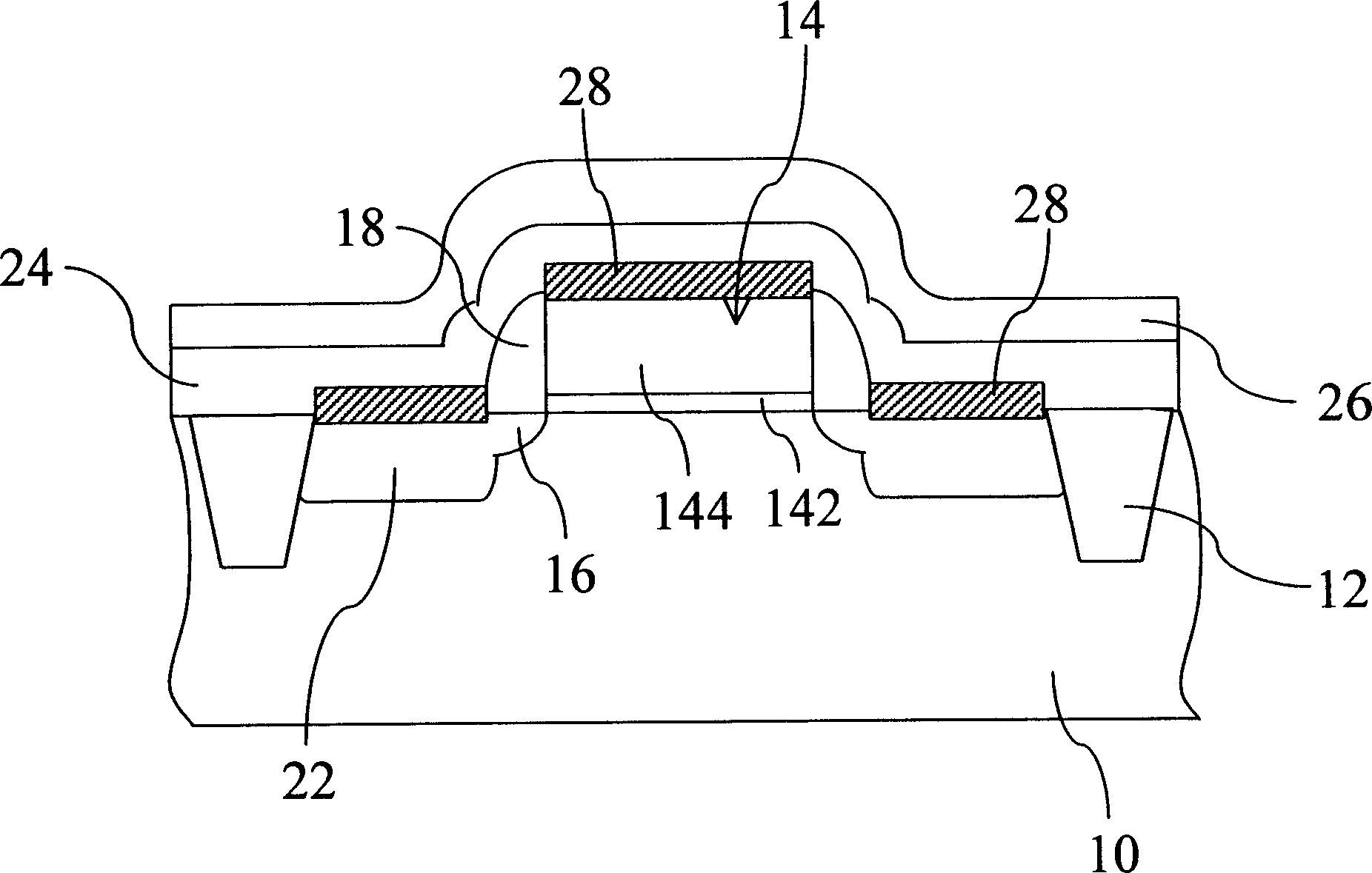
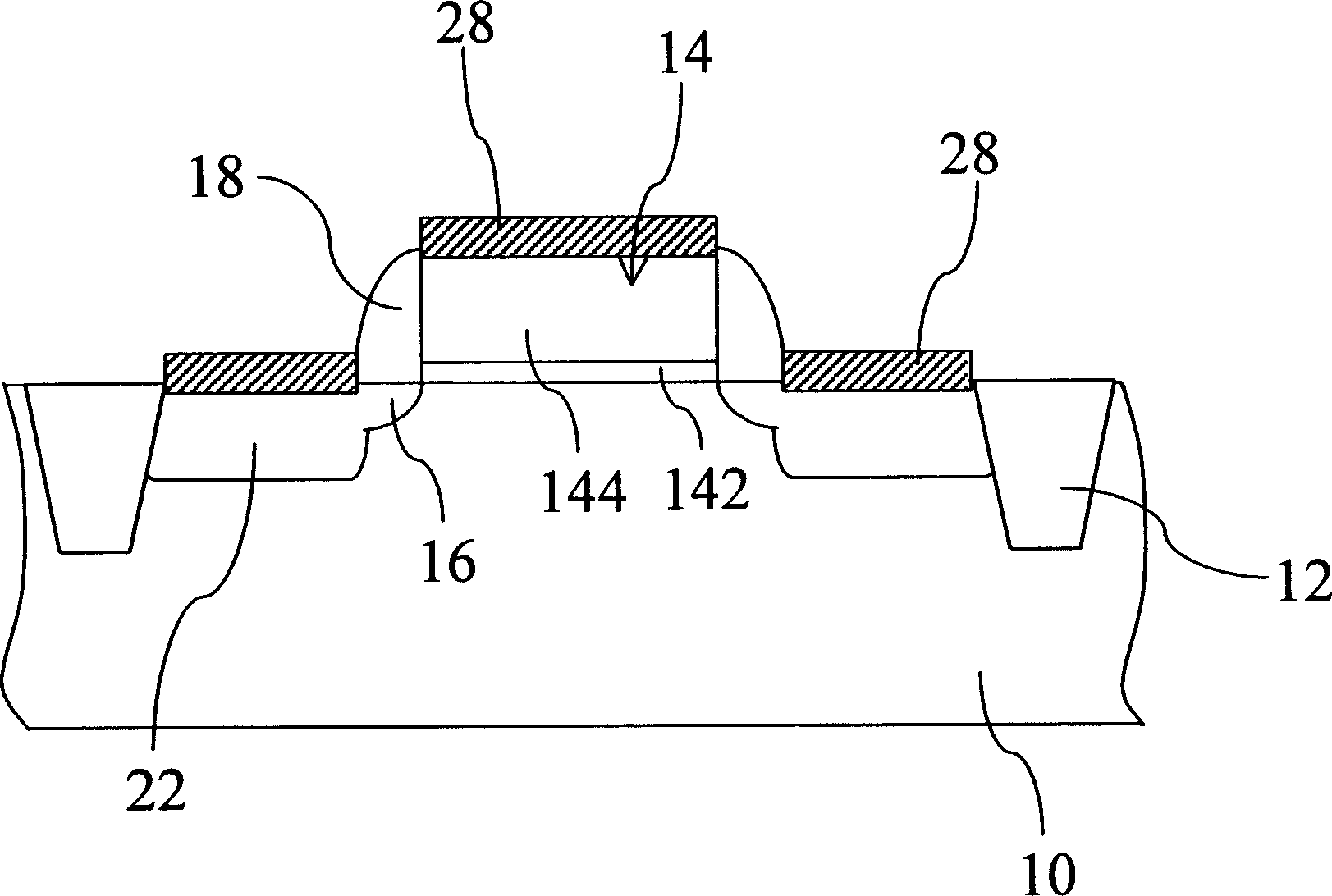
[0017] Figure 2(a) to Figure 2(f) For a preferred embodiment of the present invention, it is a cross-sectional view of each step of making a semiconductor assembly; as shown in the figure, the main manufacturing method of the present invention includes the following steps: first, as shown in Figure 2 (a), a semiconductor substrate 30 is provided , forming a shallow trench isolation region (shallow trench isolation, STI) 32 in the semiconductor substrate 30 to isolate active components and passive components in the semiconduct...


PUM

PropertyMeasurementUnit
thicknessaaaaaaaaaa

Abstract

An Isolated area, grid structure and light dope area of source/drain electrodes as well as grid gap wall and heavily doped area of source/drain electrodes are formed on substrate. Heat tempering, high temperature activating treatment and cleaning procedures are carried out in advance. Then silicon epitaxy layer growth procedure is carried out on source/drain electrodes. Finally, self-aligned method for preparing metallic silicide is carried out. The method prevents lattice defect occurred in growth procedure, and reduces leakage current phenomenon of module.

Description

technical field [0001] The present invention relates to a semiconductor manufacturing method technology, in particular to a manufacturing method including raised source / drain (raised source / drain) and self-aligned metal silicide (self-aligned silicide, Salicide), and can improve Method for manufacturing semiconductor components with lattice defects in silicon epitaxial layers. Background technique [0002] When the manufacturing method of semiconductor components enters the deep sub-micron manufacturing method, and the integrated circuit becomes higher and higher, the area of ​​the source / drain region is also reduced, but it will increase the contact resistance of the source / drain terminal, which cannot In order to maintain the high current driving capability of the device, in order to reduce the resistance value of the device and increase the convenience of the layout of the subsequent connecting wires, the self-aligned metal silicide technology has gradually been widely us...

Claims


Application Information

Patent Timeline
Patent Type & Authority Applications(China)
IPC IPC(8): H01L21/283H01L21/324H01L21/336
Inventor 高荣正
Owner GRACE SEMICON MFG CORP
Why Eureka
Try Eureka