

Scanning probe microscope
A technology of scanning probe and microscope, which is applied in the field of scanning probe microscope, can solve the problems of image instability, low resolution, and limited application range, and achieve the effect of reducing image distortion and preventing scratching of samples
- Summary
- Abstract
- Description
- Claims
- Application Information
AI Technical Summary
Problems solved by technology
Method used
Image

Examples
Embodiment Construction
[0022] The present invention will be further described in detail below in conjunction with the accompanying drawings.
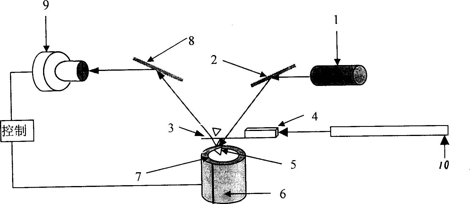
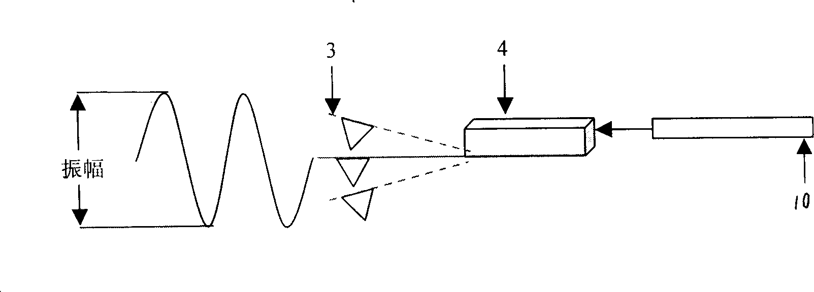
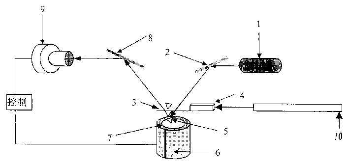
[0023] Such as figure 1 and figure 2 As shown, the scanning probe microscope of the present invention includes a laser tube 1 , a mirror 2 , a piezoelectric ceramic crystal 4 , a microcantilever 3 , a needle tip 5 , a scanning tube 6 , a mirror 8 , a spot position detector 9 , and a sample 7 . The piezoelectric ceramic crystal 4 controlled by the oscillation frequency controller 10 drives the microcantilever 3 to oscillate with a certain oscillation frequency and amplitude. When the vibration frequency of the needle tip is the same as the natural frequency of the needle tip, a resonant peak will appear, and the amplitude at this time is converted into an electrical signal by the control circuit, and the microcantilever 3 with the needle tip 5 is made to have this amplitude under the control of the control system. Oscillate on the surface of sample 7. As t...
PUM
 Abstract
Description
Claims
Application Information