Non-volatile semiconductor memory device and rewriting method

A non-volatile, storage device technology, applied in information storage, static memory, read-only memory, etc., can solve long-term problems

Inactive Publication Date: 2004-04-28
SHARP KK
View PDF4 Cites 14 Cited by
  • Summary
  • Abstract
  • Description
  • Claims
  • Application Information

AI Technical Summary

Problems solved by technology

Therefore, the above-mentioned repeated operat

Method used


Image

  • Non-volatile semiconductor memory device and rewriting method
  • Non-volatile semiconductor memory device and rewriting method
  • Non-volatile semiconductor memory device and rewriting method

Examples


Embodiment 1

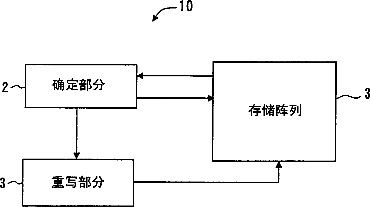
[0079] figure 1 is a block diagram showing the main part of the structure of the nonvolatile semiconductor memory device 10 according to the present invention.

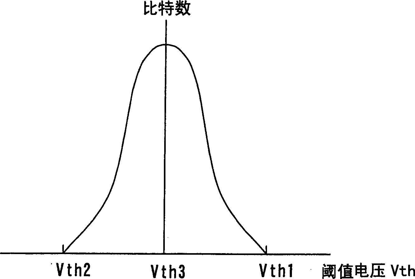
[0080] exist figure 1 Among them, the non-volatile semiconductor storage device 10 includes: a storage array 1 with a plurality of storage units, each of which can store two or more data values; whether the voltage value of the memory cell is higher or lower than a reference value preset between the maximum value and the minimum value of the voltage range corresponding to the data value; and the rewriting part 3, according to the determination result of the determination part 2, Rewriting data into the memory cell increases the margin between two adjacent voltage ranges, thereby improving data retention characteristics.

[0081] Here, the memory array 1 includes memory cell transistors as memory cells. It should be noted that the memory cells in the memory array 1 are not limited to the memory cell transistors in...

Embodiment 2

[0114] In the rewriting operation of Embodiment 1, a write signal is repeatedly applied under a specific condition. Thus, it sometimes takes a relatively long time to complete the rewriting operation. In Embodiment 2 of the present invention, an example in which the data rewriting operation is completed in a short time will be described.

[0115] In Embodiment 2, the rewriting operation of the following types of memory cells will be described. When data is read from the memory cell immediately before the rewriting operation performed in Embodiment 2, the same data value as that of the written data is read. When data is read from the memory cell after a certain period of time, due to the drift of the threshold voltage of the memory cell, a data value different from that of the written data may be read.

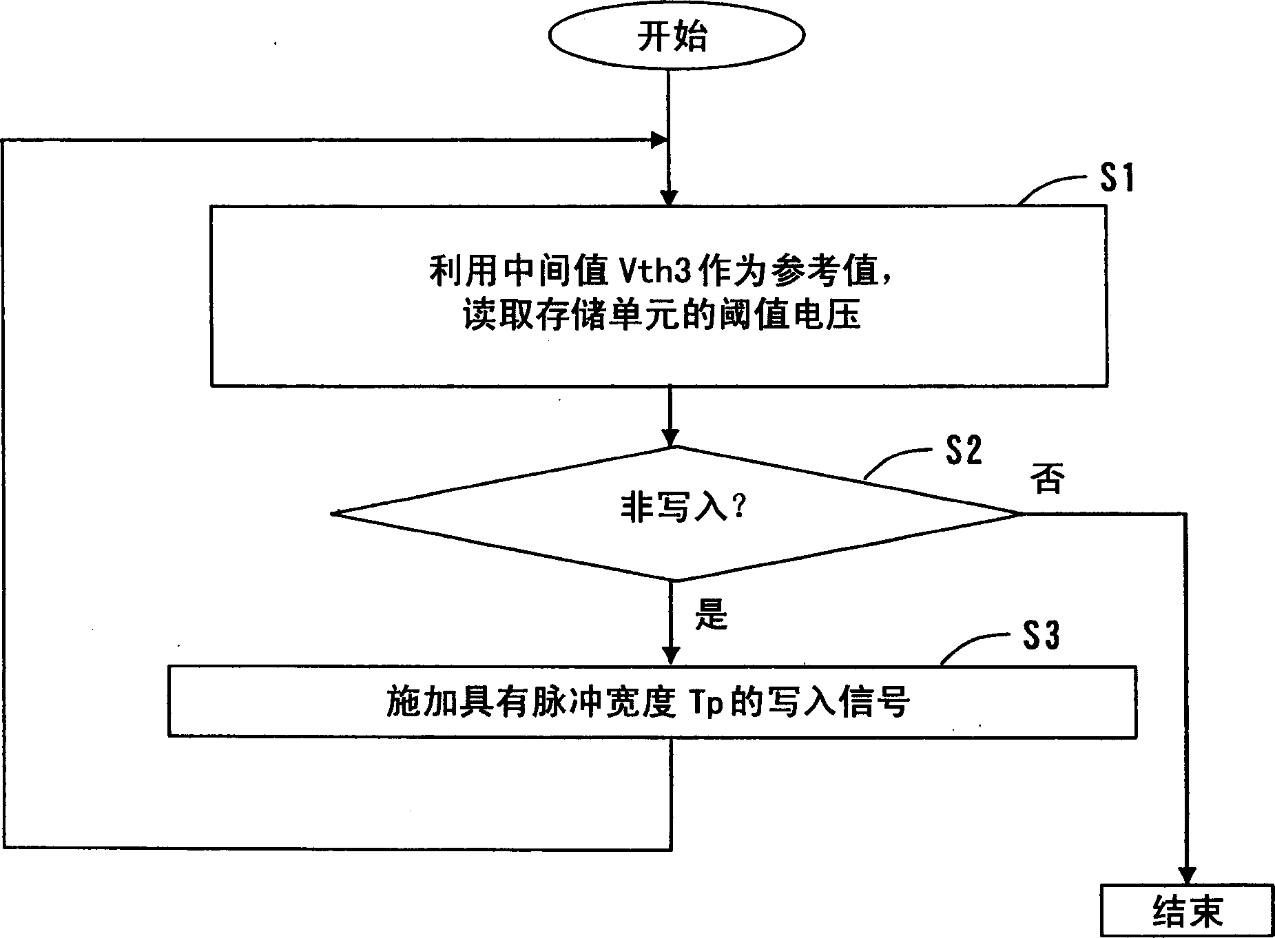
[0116] Figure 6 is a flowchart showing the procedure of the rewrite operation according to Embodiment 2 of the present invention.

[0117] In step S21, the threshold volta...

Embodiment 3

[0135] In Embodiment 3, an example in which the rewriting operation can be performed even more quickly will be described.

[0136] Same as Embodiment 2, in Embodiment 3, the rewriting operation of the following types of memory cells will be described. When data is read from the memory cell immediately before the rewriting operation performed in Embodiment 3, the same data value as that of the written data is read. When data is read from the memory cell after a certain period of time, due to the drift of the threshold voltage of the memory cell, a data value different from that of the written data may be read.

[0137] Figure 8 is a flowchart showing the procedure of the rewrite operation according to Embodiment 3 of the present invention.

[0138] In step S31, the threshold voltage of a memory cell (for example, a memory cell transistor) is read out, wherein the middle value Vth3 of the threshold voltage range corresponding to the written data value in the memory cell is us...


PUM


Abstract

A non-volatile semiconductor memory device is provided, which comprises a memory array comprising memory cells, in which each memory cell is capable of storing data values depending on the voltages thereof, the data values include a first data value corresponding to a first voltage range and a second data value corresponding to a second voltage range, and the first data is written in a memory cell of the memory cells, a determination section for determining whether a voltage value of the memory cell is higher or lower than a reference value set between a maximum value and a minimum value of the first voltage range, and a rewrite section for rewriting the first data into the memory cell based on a determination result of the determination section so that a margin between the first voltage range and the second voltage range in the memory cell is enlarged.

Description

technical field [0001] The present invention relates to a nonvolatile semiconductor storage device and a method for rewriting data into the nonvolatile semiconductor storage device. More specifically, the present invention relates to a nonvolatile semiconductor memory device suitable for multi-value flash memories such as flash EEPROM (Electrically Erasable Programmable Read Only Memory), and a method for rewriting data therein. method. Background technique [0002] Generally, electrically rewritable nonvolatile semiconductor memory devices such as EEPROM and flash EEPROM include a memory array in which a plurality of memory cell transistors are arranged, and each memory cell transistor is connected between a control gate and a semiconductor substrate. There is a charge accumulating layer between them, and the charge accumulating layer includes a floating gate and an insulating film. [0003] The threshold voltage Vth of the memory cell transistor is changed by injecting c...

Claims


Application Information

Patent Timeline
IPC IPC(8): G11C16/02G11C11/56G11C16/12G11C16/34
CPCG11C11/5628G11C16/3431G11C16/3418G11C11/5642G11C16/3404G11C16/12
Inventor 田中嗣彦
Owner SHARP KK
Why Eureka
Try Eureka