Performance-improved white organic luminescent device
A device and organic technology, applied in the field of organic light-emitting OLED devices, can solve problems such as changes in the color of emitted light and difficult process control
- Summary
- Abstract
- Description
- Claims
- Application Information
AI Technical Summary
Problems solved by technology
Method used
Image
Examples
Embodiment 1
[0191] The device of Example 1 was prepared by sequentially depositing a 150 nm NPB hole transport layer (HTL), a 20 nm blue light emitting layer (LEL) of a TBADN matrix containing 2% TBP blue dopant, a 37.5 nm Alq electron transport layer (ETL), and then 0.5nm LiF and 200nm Al as part of the cathode. The above sequence completes the deposition of the OLED device.
[0192] Then the OLED device was sealed and packaged in a nitrogen-filled dry glove box to isolate the surrounding environment. The ITO patterned substrates used to fabricate OLED devices included several experimental patterns. Each device was tested for its volt-ampere characteristic curve and electroluminescence yield.
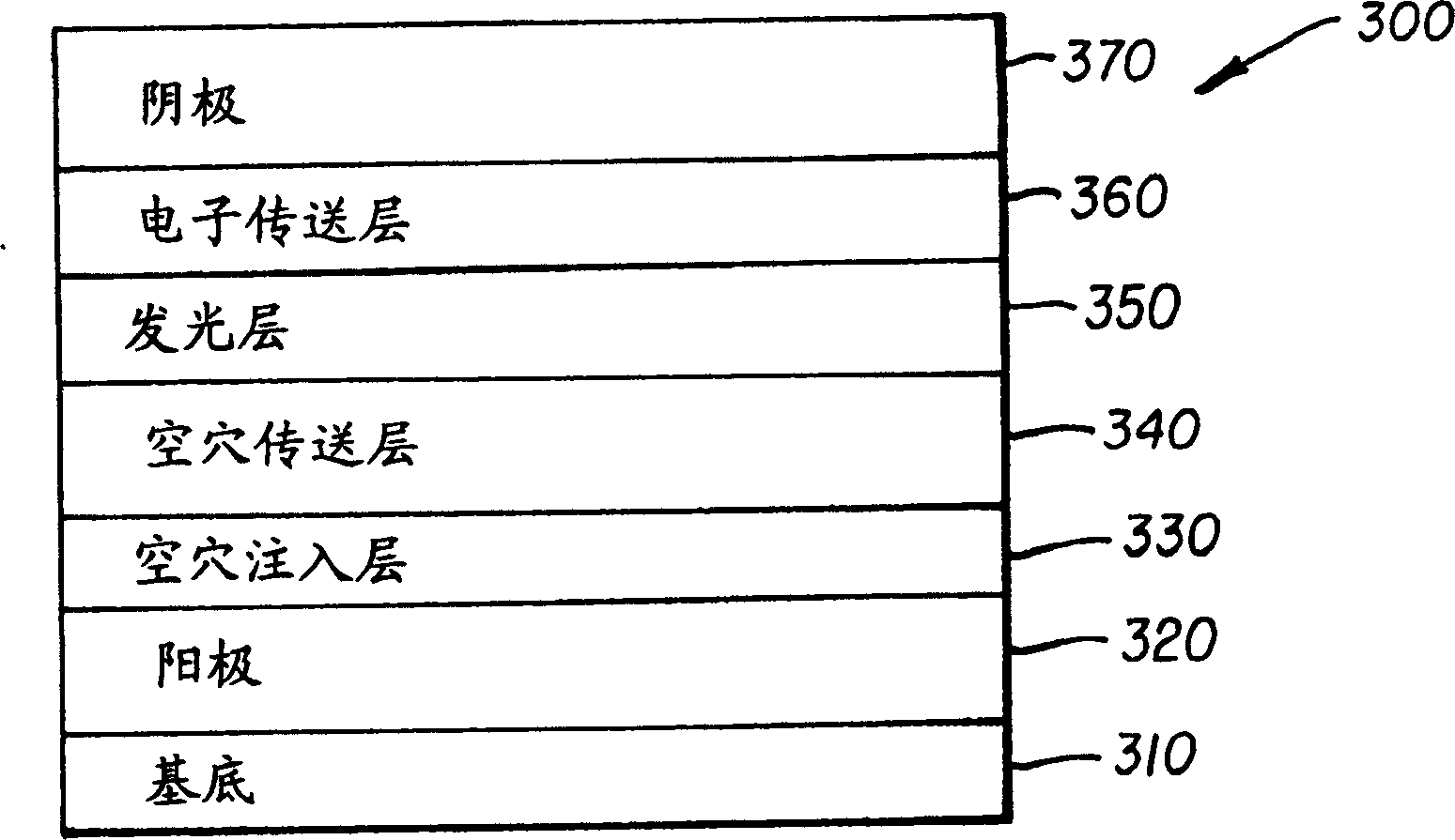
[0193] according to image 3 Devices of Examples 2-6 were prepared with the structure of OLED 300 shown in . A 150 nm thick NPB hole transport layer was doped with varying amounts of rubrene at a concentration of 1-5%. The device of Example 1 was found to have emission in the blue region of t...
PUM
 Abstract
Description
Claims
Application Information


