Plasma display panel and its manufacturing method
A plasma and manufacturing method technology, applied in the direction of AC plasma display panels, cold cathode manufacturing, electrode system manufacturing, etc., can solve the problems of reduced luminous efficiency, etc., and achieve the effect of reducing equipment costs and excellent luminous efficiency
- Summary
- Abstract
- Description
- Claims
- Application Information
AI Technical Summary
Problems solved by technology
Method used
Image

Examples
Embodiment 1
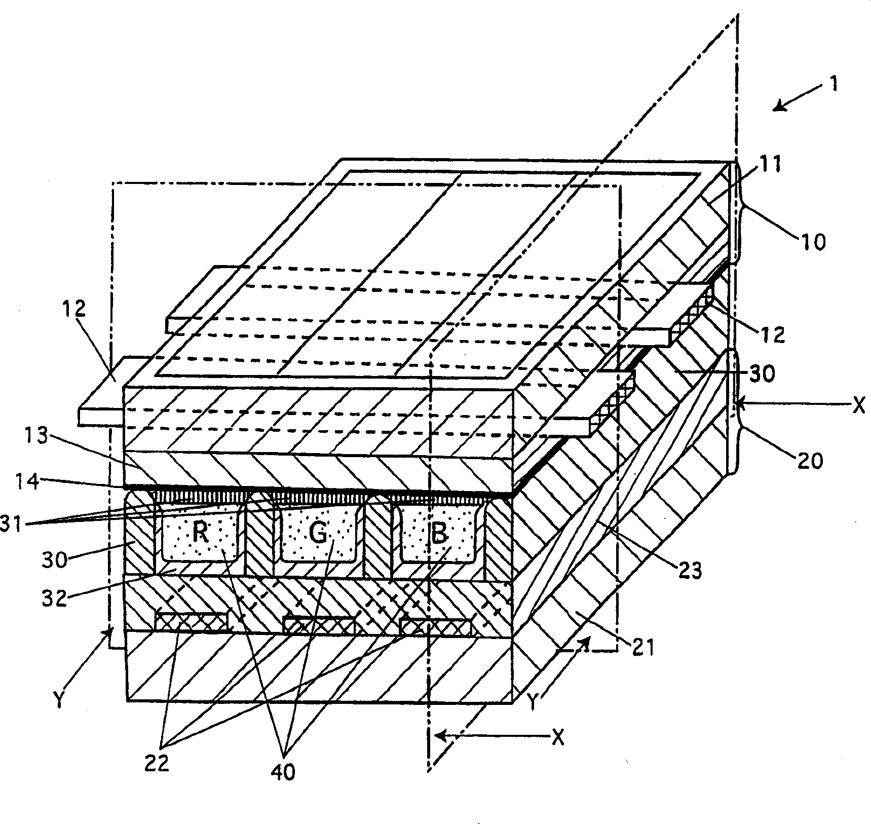
[0066] 1. The overall structure of the screen
[0067] use figure 1 The overall structure of the AC-type PDP of Example 1 will be described. figure 1 is a diagram showing part of the AC-type PDP1.
[0068] Such as figure 1 As shown, the AC-type PDP 1 has a structure in which a front panel 10 and a rear panel 20 are arranged to face each other with a certain distance therebetween, and the space between the panels is divided into a plurality of discharge spaces 40 by barrier ribs 30 .
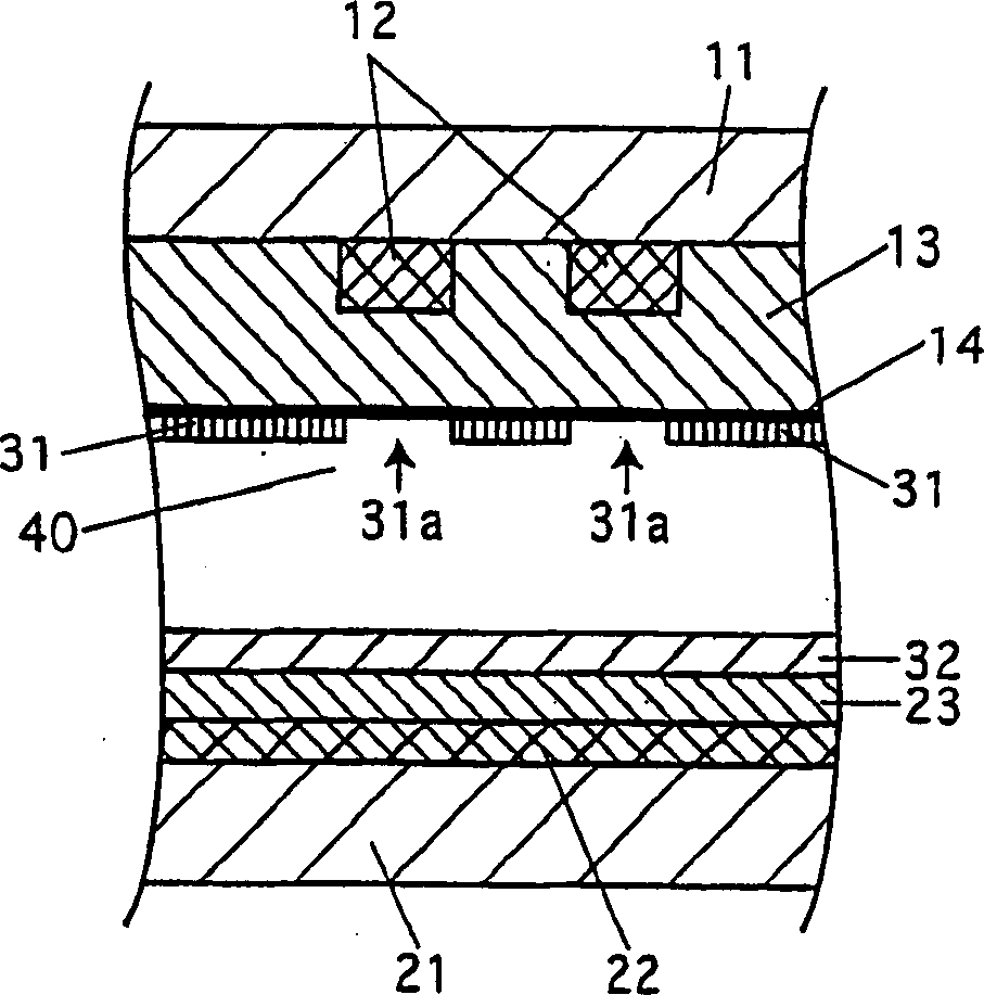
[0069] The front panel 10 has a structure in which a plurality of display electrodes 12 are arranged in stripes on one main surface (lower side in the figure) of a front glass substrate 11, and a first dielectric layer 13 and a dielectric protective film are sequentially stacked on this surface. 14.
[0070] A plurality of address electrodes 22 are arranged in stripes on the rear glass substrate 21 facing the front panel 10 of the rear panel 20, and then a second dielectric layer 23 coveri...
Embodiment 2
[0162] use Figure 13 The AC-type PDP2 of Example 2 will be described. Figure 13 A cross-sectional view of an AC-type PDP 2 corresponding to only one light-emitting unit is shown.
[0163] Such as Figure 13 As shown, the phosphor film (layer) formed in the AC type PDP 2 is only the first phosphor film 31 formed on the surface of the front panel 10 . That is, no phosphor film (layer) is formed on the rear panel 20 and barrier ribs 30 .
[0164] Except for this point, the AC-type PDP2 has the same structure as the above-mentioned AC-type PDP1, and is manufactured by the same method.
[0165] In addition, the point that the first phosphor film 31 has a notch 31a is also the same as that of the above-mentioned AC type PDP 1 (not shown).
[0166] The AC-type PDP 2 can obtain sufficiently high luminance without forming a phosphor layer composed of conventional phosphor particle groups on the surfaces of the rear panel 20 and the barrier ribs 30 . As described above, this is p...
Embodiment 3
[0173] use Figure 15 The AC-type PDP3 of Example 3 will be described.
[0174] Such as Figure 15 As shown, the AC-type PDP3 and the above-mentioned AC-type PDP2 only form the first phosphor film 31 on the front panel 10, which is the same. The difference is that the address electrodes 22 and the second dielectric layer are formed on the front panel 10. 23 , forming the display electrodes 12 , the first dielectric layer 13 and the dielectric protection film 14 on the rear panel 20 .
[0175]When this structure is adopted, in order not to affect the transmission of visible light, the address electrodes 22 and the second dielectric layer 23 are formed of materials with high transmittance of visible light. Specifically, the address electrode 22 uses ITO (Indium Tin Oxide) and SnO 2 and other transparent electrodes, the second dielectric layer 23 is made of lead glass mainly composed of lead oxide. Because the address electrode 22 is formed on the short side direction of the ...
PUM
 Abstract
Description
Claims
Application Information
 - R&D Engineer
- R&D Manager
- IP Professional
- Industry Leading Data Capabilities
- Powerful AI technology
- Patent DNA Extraction
Browse by: Latest US Patents, China's latest patents, Technical Efficacy Thesaurus, Application Domain, Technology Topic.
© 2024 PatSnap. All rights reserved.Legal|Privacy policy|Modern Slavery Act Transparency Statement|Sitemap