Electro-optical device and electronic equipment

一种电光装置、遮光层的技术,应用在光学、非线性光学、静态指示器等方向,能够解决延迟值不均匀、不能应用反射半透过型面板、基板间隔不均匀等问题,达到光照射效率提高、促进结晶化效率的效果

Inactive Publication Date: 2004-05-19
SEIKO EPSON CORP
View PDF3 Cites 6 Cited by
  • Summary
  • Abstract
  • Description
  • Claims
  • Application Information

AI Technical Summary

Problems solved by technology

As described in Patent Document 1, if the light-shielding film is formed only corresponding to the formation region of the TFT element, there will be a step difference on the element substrate due to the formation region and the non-formation region, and the substrate spacing will become uneven in each region, and there will be The problem of uneven delay value
In addition, as described in Patent Document 2, the structure in which a light-shielding layer is provided on the substantially front surface of the TFT element substrate on the liquid crystal side cannot be applied to a transflective panel.
In addition, as described in Patent Document 3, the structure of providing a light-shielding layer on the source (electrode) line cannot be applied to a transflective panel.

Method used


Image

  • Electro-optical device and electronic equipment
  • Electro-optical device and electronic equipment
  • Electro-optical device and electronic equipment

Examples


Embodiment Construction

[0032] Hereinafter, embodiments of the present invention will be described with reference to the drawings.

[0033] Electro-optic device

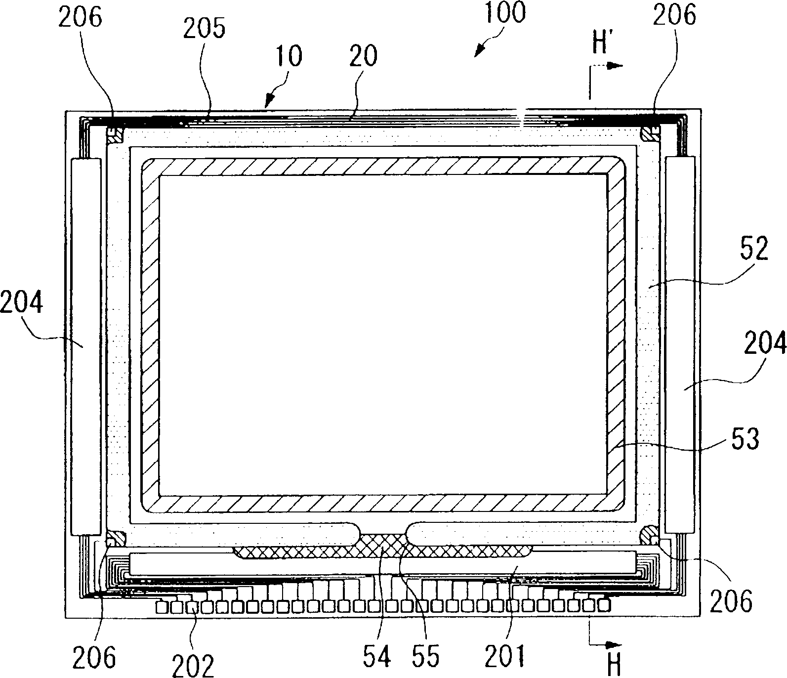
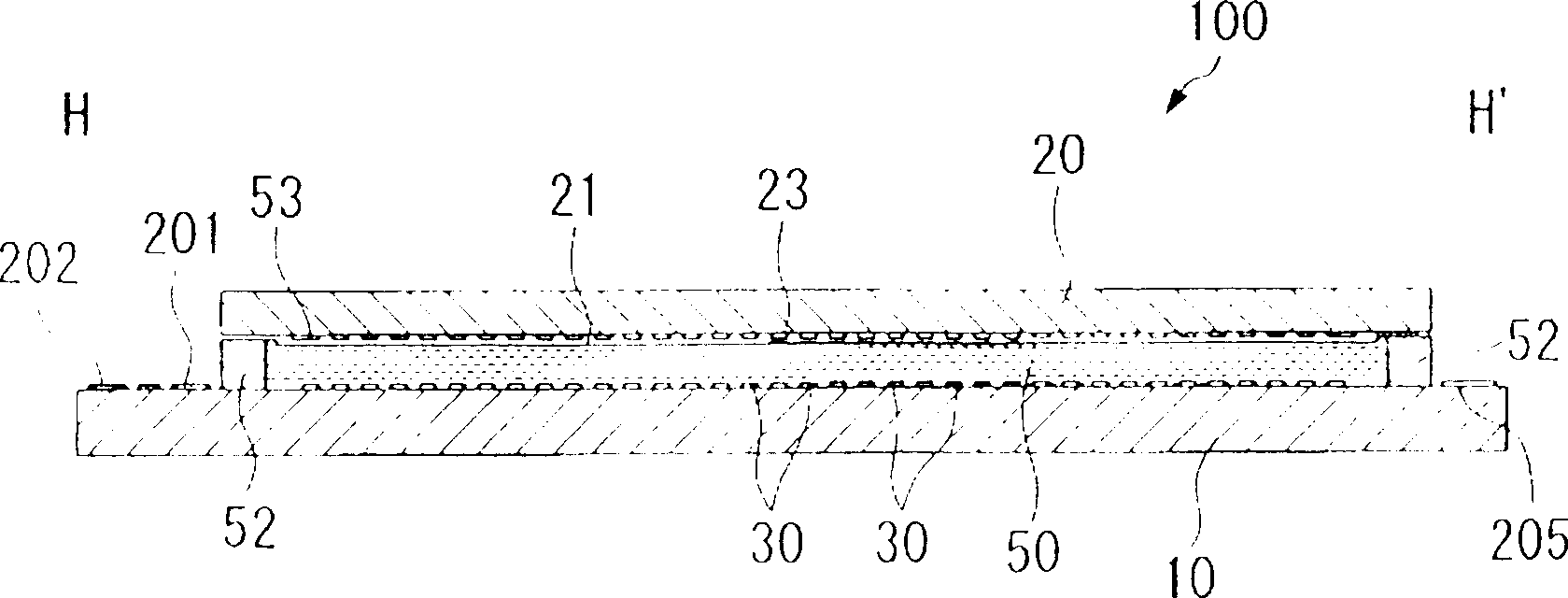
[0034] figure 1 It is an embodiment of the electro-optic device of the present invention, and is a plan view of a liquid crystal display device using liquid crystal as an electro-optic material, which is displayed together with each constituent element and viewed from the counter substrate side, figure 2 is along figure 1 Sectional view of the H-H' line.

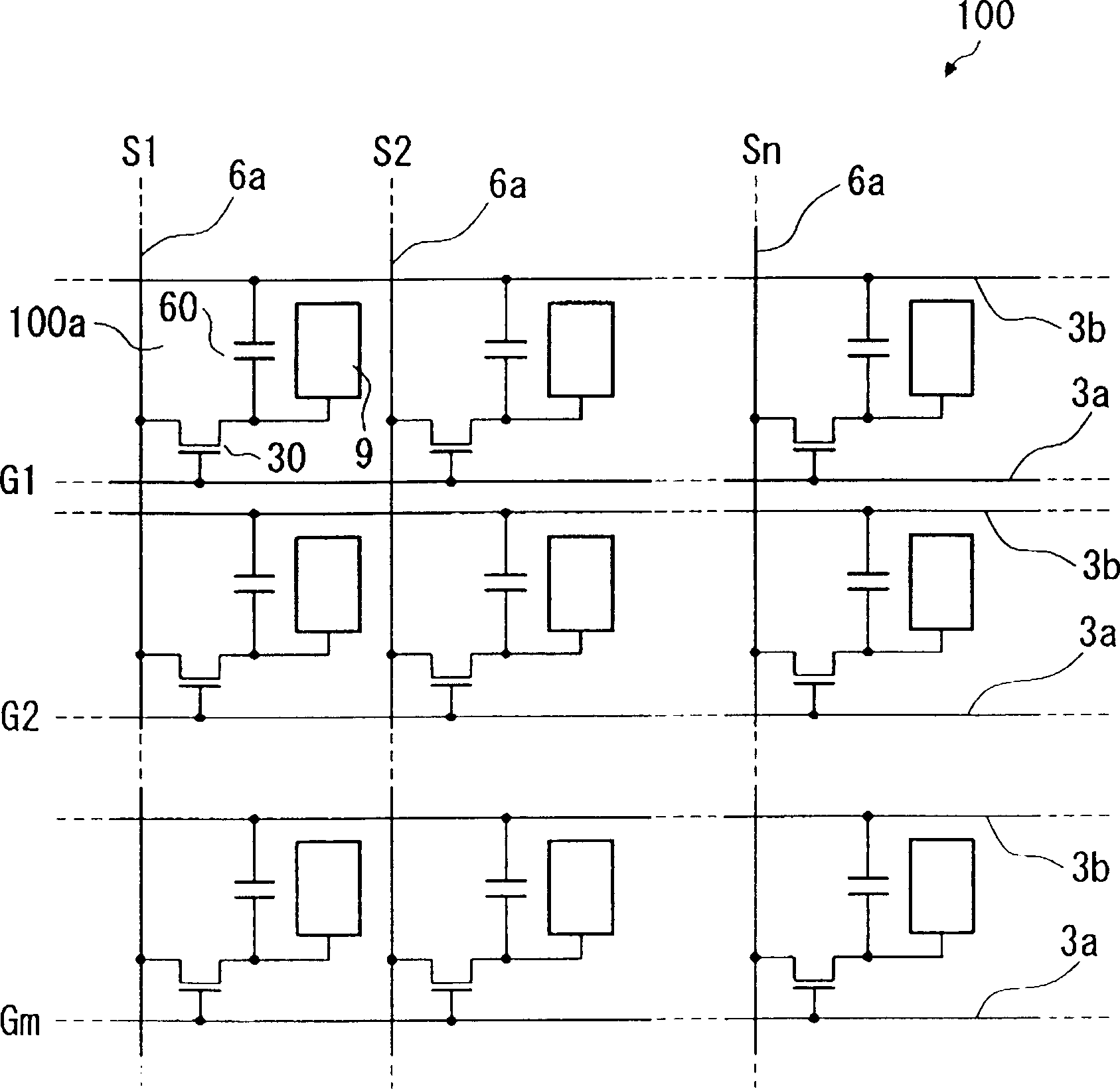
[0035] image 3 It is an equivalent circuit diagram of various elements, wiring (wiring), etc. in a plurality of pixels formed in a matrix in the image display area of ​​the liquid crystal display device, Figure 4 is a partially enlarged plan view showing the configuration of each pixel of a liquid crystal display device, Figure 5 yes Figure 4 Cross-sectional view of A-A'.

[0036] Furthermore, in each drawing used in the following description, in order to make each layer and eac...


PUM


Abstract

The object of the present invention is to provide a photoelectric device capable of effectively utilizing a light shielding layer for preventing control light from injecting to a semiconductor device. To achieve the object, the inventive liquid crystal display device is characterized in comprising: photoelectric material 50 sandwiched between a device substrate 10 of pixel electrode 9 and a counter substrate 20 opposite to the device substrate 10. The device substrate 10 includes: a semiconductor device 30 for driving the pixel electrode 9, insulating films 17 and 18 covering the semiconductor device 30, and a reflective plate 14 formed on the insulating films 17 and 18. The reflective plate 14 has an opening 14a. On the other hand, a light shielding layer 13 for shielding the light injecting to the semiconductor device 30 is formed on the side of device substrate 10 of the semiconductor device 30. The light shielding layer 13 has an opening 13a at substantially the same region as the opening 14a of the reflective plate 14.

Description

technical field [0001] The present invention relates to an electro-optical device and an electronic device including the electro-optical device, and particularly to a transflective (transmissive) reflective electro-optic device having a reflection plate on the inner surface of a substrate. Background technique [0002] As a conventionally known electro-optical device such as a liquid crystal device, an electro-optic material such as liquid crystal is sandwiched (interposed) between a pair of substrates, and at the same time, matrix-shaped pixel electrodes are formed on the substrates, and the pixel electrodes are controlled by TFT elements. An active-matrix type display device that can perform on-off display by power-on control. In a display device using such a TFT element, when light enters a channel region of the TFT element, an optical leakage current is generated, which may cause display defects such as a decrease in contrast and screen flickering. Therefore, for exampl...

Claims


Application Information

Patent Timeline
Patent Type & Authority Applications(China)
IPC IPC(8): G02F1/1333G02F1/1335G02F1/1362G02F1/1368
CPCG02F1/133553G02F1/133555G02F1/136227G02F1/136209G02F1/1335
Inventor 关琢巳北川篤史
Owner SEIKO EPSON CORP
Why Eureka
Try Eureka