Organic luminescent device with enhanced light extraction efficiency

A light extraction and device technology, applied in organic semiconductor devices, semiconductor devices of light-emitting elements, electric solid devices, etc., can solve problems such as incompatibility

Inactive Publication Date: 2004-05-19
EASTMAN KODAK CO
View PDF58 Cites 61 Cited by
  • Summary
  • Abstract
  • Description
  • Claims
  • Application Information

AI Technical Summary

Problems solved by technology

However, the general problem encountered by all these methods is that the complexity of the device structure is greatly increased, and at the same time, the generated light output has a high degree of dependence on angle and wavelength, which is not suitable for many practical applications.
The efficiency of OLED devices is thus improved, but defects remain

Method used


Image

  • Organic luminescent device with enhanced light extraction efficiency
  • Organic luminescent device with enhanced light extraction efficiency
  • Organic luminescent device with enhanced light extraction efficiency

Examples


Embodiment Construction

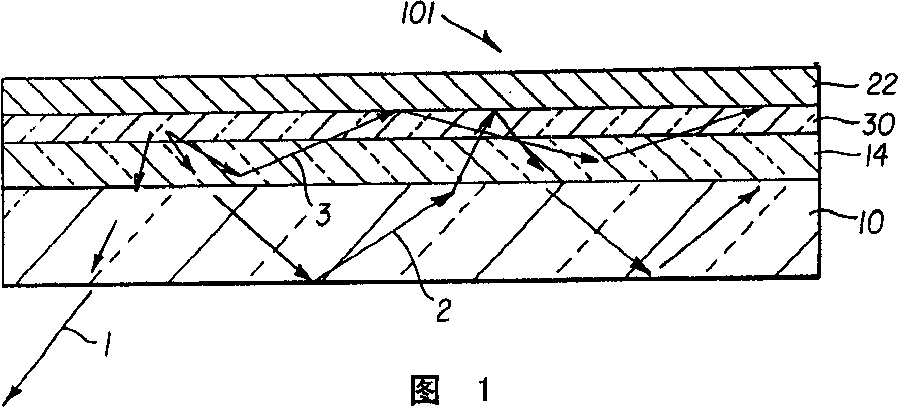
[0032] FIG. 1 is a schematic cross-sectional view of a typical common OLED device 101 . The device 101 includes a substrate 10 , an anode layer 14 , an organic EL element 30 and a cathode layer 22 . The organic EL element 30 may contain one or more sublayers, including a hole injection layer, a hole transport layer, a light emitting layer, an electron transport layer, and an electron injection layer. Most generally, substrate 10 and anode layer 14 are transparent, cathode layer 22 is reflective, and light generated from the device is emitted through anode layer 14 and substrate 10 . This is often referred to as a bottom emitting OLED device. OLED devices can also be top emitting. In a top emitting OLED device, the anode layer is made reflective and the cathode layer is made transparent, and the generated light is emitted through the cathode layer. The discussion below based on bottom-emitting devices also applies to top-emitting devices. Additionally, the order of the layer...


PUM

PropertyMeasurementUnit
electron work functionaaaaaaaaaa

Abstract

An enhanced light extraction OLED device including a transparent substrate; light scattering layer disposed over a first surface of the transparent substrate; a transparent first electrode layer disposed over the light scattering layer; an organic EL element disposed over the transparent first electrode layer and including one or more organic layers but at least one light emitting layer in which light is produced; and a transparent second electrode layer disposed over the organic EL element.

Description

technical field [0001] The present invention relates to organic light emitting diodes (OLEDs) having enhanced light extraction efficiency and suitable for use as light sources and displays. Background technique [0002] Organic light emitting devices (OLEDs) generally come in two forms, known as small molecule devices as disclosed in commonly assigned US-A-4,476,292 and polymeric OLED devices as disclosed in US-A-5,247,190. Each type of OLED device may sequentially contain an anode, an organic EL element, and a cathode. An organic EL element positioned between an anode and a cathode generally includes an organic hole transport layer (HTL), an emission layer (EL), and an organic electron transport layer (ETL). Holes and electrons recombine in the EL layer and emit light. Tang et al. (Appl. Phys. Lett., 51, 913 (1987), Journal of Applied Physics, 65, 3610 (1989) and commonly assigned US-A-4,476,292) reported highly efficient OLEDs. Since then, a large number of OLEDs conta...

Claims


Application Information

Patent Timeline
Patent Type & Authority Applications(China)
IPC IPC(8): H05B33/02F21K99/00H01L51/00H01L51/30H01L51/50H05B33/14H05B33/22H05B33/24
CPCH01L51/005H01L51/0037H05B33/14H01L51/0081H05B33/24H01L51/5268H01L51/0035H01L51/0077H01L51/0059Y02B20/383H01L51/5271H01L2251/5338F21K9/135H01L51/0052H01L51/0036F21Y2101/02F21Y2105/008H01L2251/5361H01L51/0042F21Y2105/00F21K9/232F21Y2115/15H10K85/111H10K85/1135H10K85/146H10K85/60H10K85/113H10K85/615H10K85/631H10K85/30H10K85/324H10K50/854H10K50/856H10K2102/311H05B33/22
Inventor 田元生邓青云廖良生
Owner EASTMAN KODAK CO
Why Eureka
Try Eureka