Semiconductor memory apparatus and data write method

A data writing and memory technology, applied in the direction of static memory, read-only memory, digital memory information, etc., can solve the problem of prolonging time

Inactive Publication Date: 2004-07-07
异基因开发有限责任公司
View PDF2 Cites 6 Cited by
  • Summary
  • Abstract
  • Description
  • Claims
  • Application Information

AI Technical Summary

Problems solved by technology

Therefore, using the above method to write data into each memory cell of the flash memory will significantly prolong the time required to complete the data write operation (programming)

Method used


Image

  • Semiconductor memory apparatus and data write method
  • Semiconductor memory apparatus and data write method
  • Semiconductor memory apparatus and data write method

Examples


Embodiment Construction

[0073] Hereinafter, the present invention will be described by way of schematic examples and with reference to the accompanying drawings.

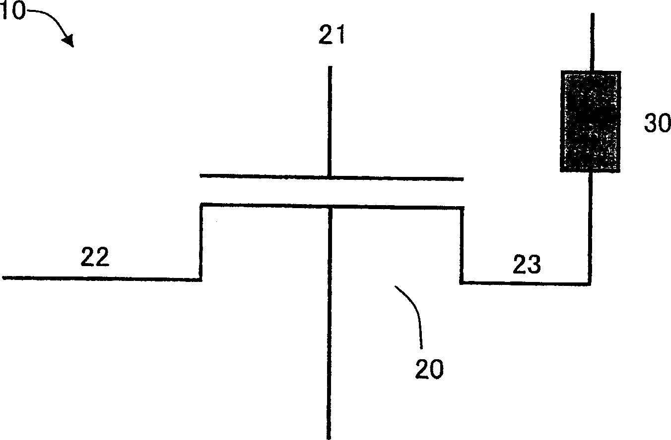
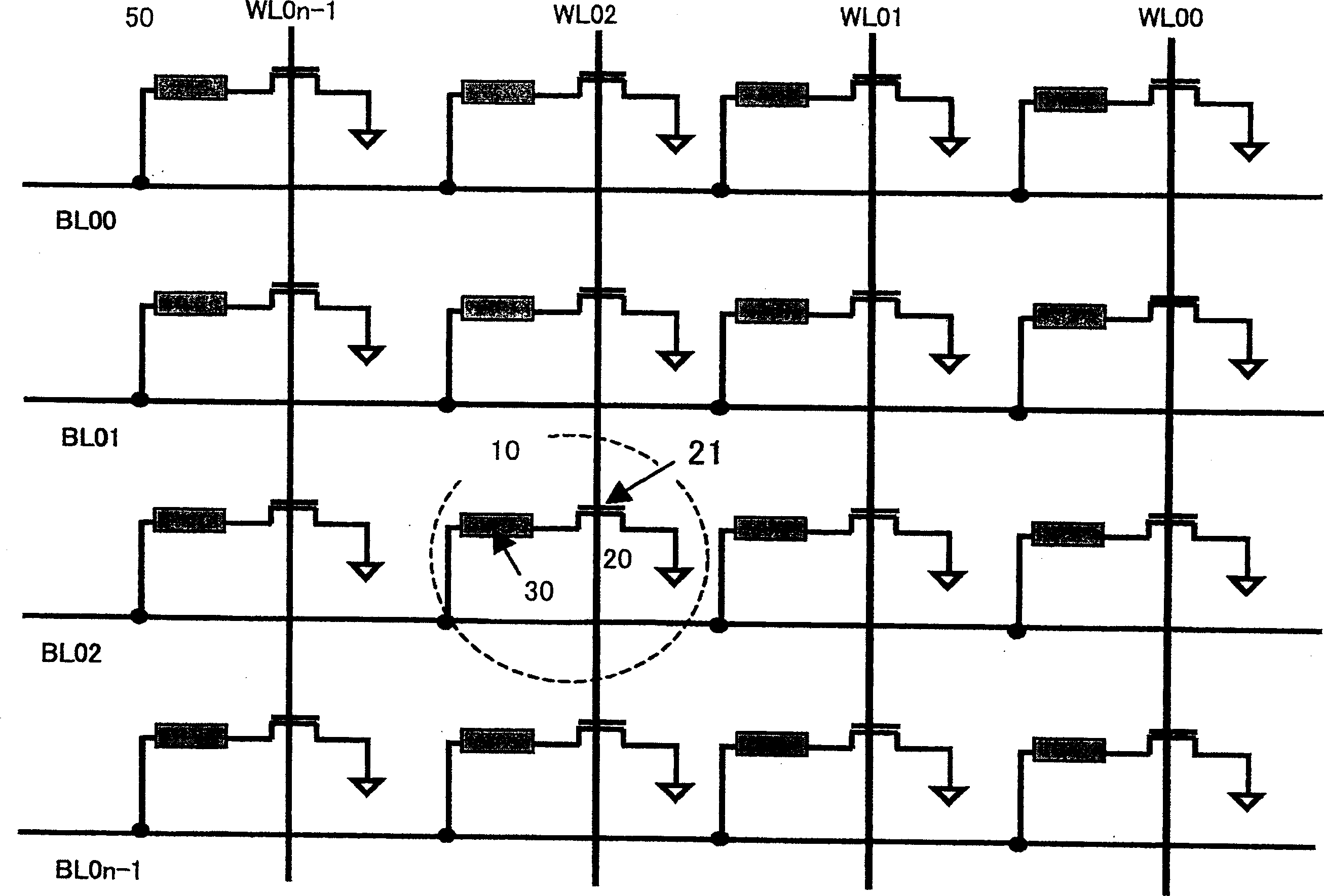
[0074] figure 1 is a schematic diagram of a nonvolatile semiconductor memory cell (hereinafter referred to as "memory cell") 10 included in the semiconductor memory device according to the present invention.

[0075]The memory cell 10 comprises a transistor having a gate electrode 21 , a source region 22 and a drain region 23 , and a variable resistor 30 connected to the drain region 23 as a memory carrier. Transistors and variable resistors 30 are formed on a semiconductor substrate (not shown). Here, the transistors are MOS transistors.

[0076] The variable resistor 30 , which is a memory carrier corresponding to the memory cell 10 , has a resistance value that can be continuously and reversely changed by a voltage applied between both ends of the variable resistor 30 or voltages. Even after the voltage application is terminated, th...


PUM


Abstract

A semiconductor memory device including a plurality of memory cells is provided. One of the plurality of memory cells includes a variable resistor having a resistance value thereof reversibly changed in accordance with a voltage applied thereto, and a transistor connected to the variable resistor.

Description

technical field [0001] The present invention relates to a semiconductor memory device and a data writing method, and in particular to a semiconductor memory device including a plurality of memory cells and a method for writing data to such a semiconductor memory device. Background technique [0002] Recently, semiconductor memory devices such as nonvolatile memories have been significantly improved in performance such as degree of integration, data processing rate, and the like. In particular, flash memory, as a nonvolatile memory, is widely used in dense information devices such as personal terminals such as cellular phones. Flash memory is a type of EEPROM (Electrically Erasable Programmable Read Only Memory). Flash memory includes a plurality of memory cells. Each memory cell includes a MOS transistor with a floating gate that is electrically isolated from other elements in the memory cell. [0003] Figure 8 is a schematic cross-sectional view of a memory cell 100 inc...

Claims


Application Information

Patent Timeline
Patent Type & Authority Applications(China)
IPC IPC(8): G11C16/00G11C11/56G11C13/00G11C16/02G11C16/10G11C16/34
CPCG11C13/0069G11C11/5685G11C2213/79G11C2213/31G11C13/0007G11C16/3413G11C13/0097G11C2013/0073G11C13/0064G11C16/00
Inventor 森本英德井上刚至
Owner 异基因开发有限责任公司
Why Eureka
Try Eureka