High-speed in-line electro-optics testing method and system for defects on chip

An electro-optical detection and defect technology, applied in the field of methods and systems, can solve problems such as time spent on detecting wafers

Inactive Publication Date: 2010-05-12
NEGEFF TECH
View PDF8 Cites 0 Cited by
  • Summary
  • Abstract
  • Description
  • Claims
  • Application Information

AI Technical Summary

Problems solved by technology

Although the system can simultaneously acquire a 2D image of the inspected object, it is very time-consuming to inspect the entire wafer

Method used


Image

  • High-speed in-line electro-optics testing method and system for defects on chip
  • High-speed in-line electro-optics testing method and system for defects on chip
  • High-speed in-line electro-optics testing method and system for defects on chip

Examples


Embodiment Construction

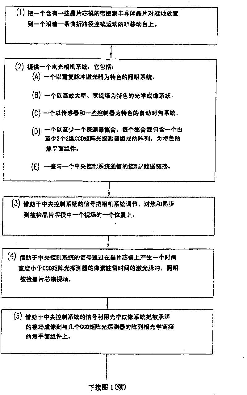
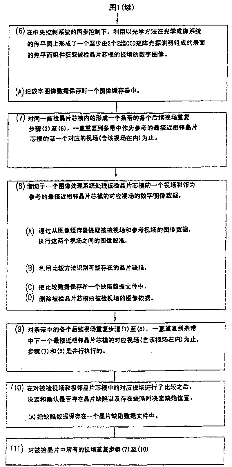
[0046] The present invention advantageously includes methods and systems for rapid in-line electro-optic detection of wafer defects.

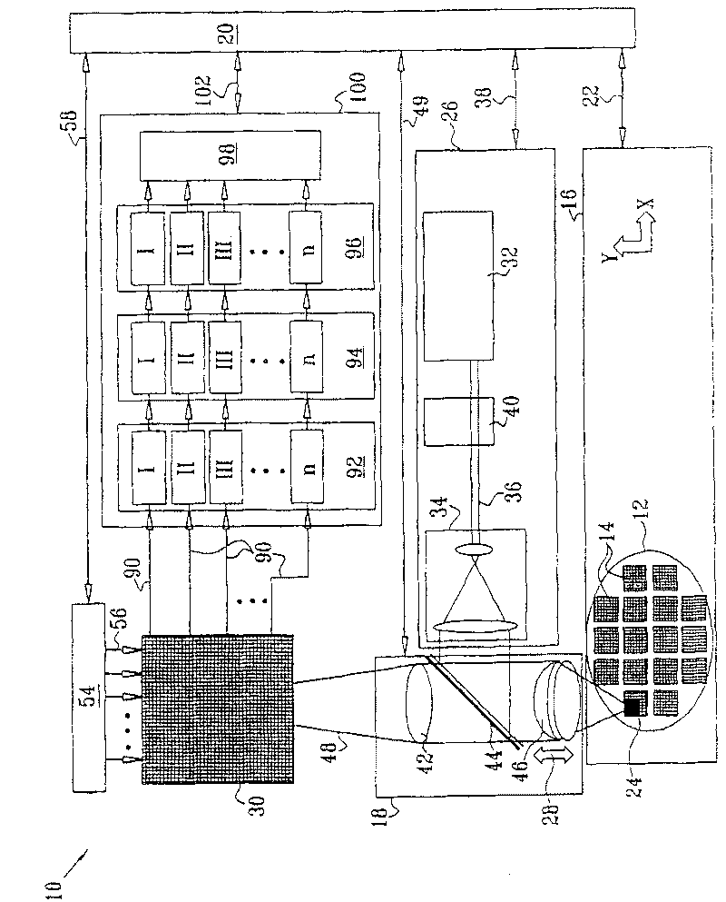
[0047] The method and system for rapid on-line electro-optic detection of wafer defects of the present invention introduce a unique combination of a new imaging system and an illumination system, wherein the new imaging system is characterized by an optical method formed on a surface composed of several 2-dimensional matrix photodetectors. The photodetector surface on the focal plane formed by the composed array is used to acquire high resolution, high pixel density and large field of view images of the wafer die in synchronization with the illumination system; the illumination system is characterized by the use of a repeating Short pulses of light from a pulsed laser illuminate the wafer die. The width of the laser pulse is much shorter than the dwell time of the image pixel, where the pixel dwell time refers to the time when a point on the wa...


PUM


Abstract

An electrooptical method and system for high-speed in-line inspection of defects on chip features that the short light pulses from a repetition pulse laser device are used to radiate the visual fieldsof an electrooptical camera system with a microscopic optical system and a moving chip is imaged on a focal plane module, which can optically generate an optical detector surface on the focal plane of optical imaging system. Said surface is composed of 6 detector sets. Each set has an array consisting of 4 2D CCD-matrix optical detectors. Each 2D CCD-matrix detector can generate an electronic image containing 2M pixels. All said electronic images generated by said 4 detectors can be simultaneously processed and compared with a reference image to find out any defects.

Description

technical field [0001] The present invention relates to methods and systems for electro-optical detection of random manufacturing defects in semiconductor patterned structures such as semiconductor wafers as integrated circuit dies or chips. Background technique [0002] In particular, the present invention relates to a method and system for rapid on-line detection of wafer defects in which a short light pulse from a pulsed laser illuminates the field of view of an electro-optic camera system with a micro-optic system, and a The moving wafer is imaged onto a focal plane assembly (FPA), which optically forms a photodetector surface at the focal plane of an optical imaging system consisting of several detector sets, each detector set Both comprise an array of several 2-dimensional matrix photodetectors, each of which produces an electronic image in the form of a matrix of pixels, so that the method and system can use conventional image processing techniques to analyze images m...

Claims


Application Information

Patent Timeline
Patent Type & Authority Patents(China)
IPC IPC(8): H01L21/66
Inventor 加德·诺伊曼
Owner NEGEFF TECH
Why Eureka
Try Eureka