

Luminous diplay panel and its mfg. method
A technology of luminous display and manufacturing method, which is applied in electroluminescent light sources, semiconductor/solid-state device manufacturing, optics, etc., can solve problems such as difficult to see the display of luminescent display panels, and achieve the effect of not being easily damaged
- Summary
- Abstract
- Description
- Claims
- Application Information
AI Technical Summary
Problems solved by technology
Method used
Image

Examples
Embodiment 1
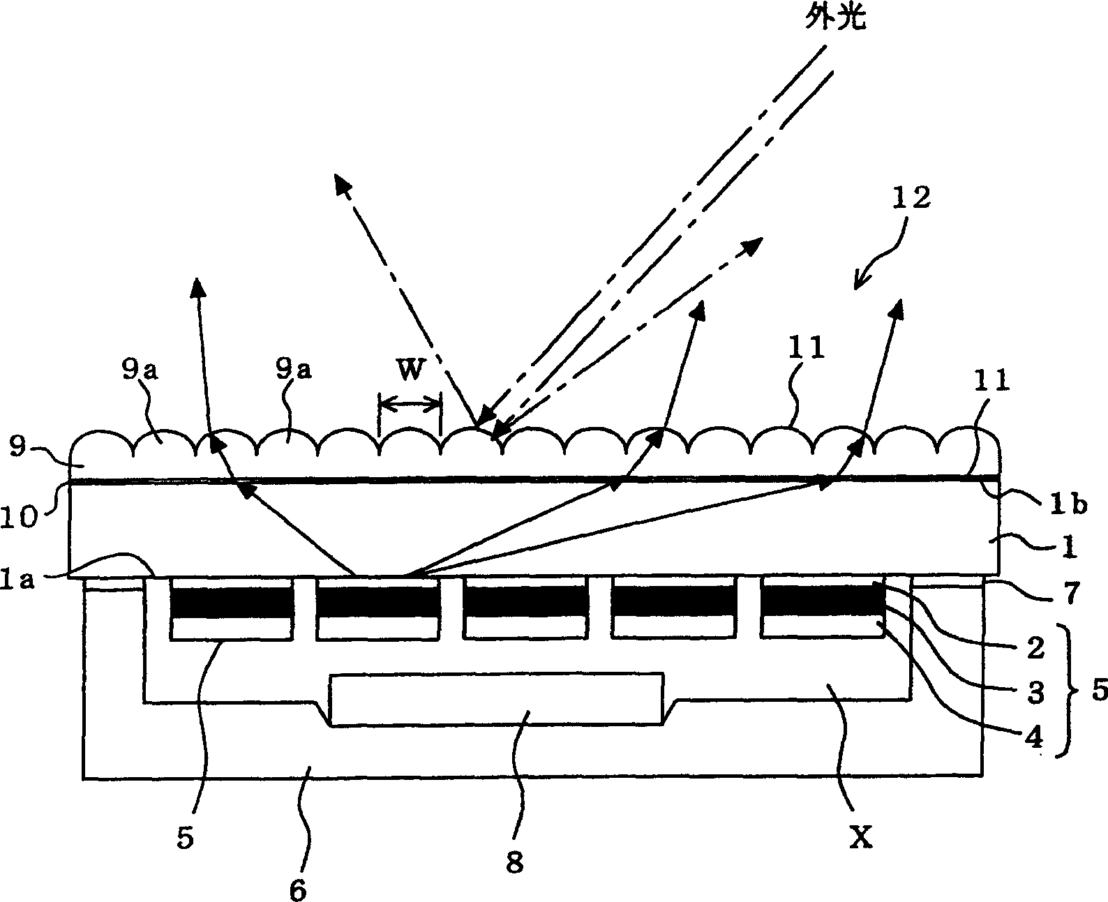
[0030] figure 1 It is an explanatory view of the structure represented by the cross-section of Example 1 of the present invention. In the figure, 1 is a transparent substrate made of glass, and a plurality of transparent electrodes such as indium tin oxide (Indium Tin Oxide, hereinafter referred to as "ITO") are sequentially stacked on one surface (lower surface) 1a. A light-emitting element (organic EL element) 5 formed of a single-layer or multi-layer organic EL material layer 3 and a metal electrode 4 including at least a light-emitting functional layer. The sealing material around each light-emitting element 5 on the side of the lower surface 1a can prevent, for example, deterioration of light-emitting characteristics of the light-emitting element 5 made of glass due to moisture. 8 is a drying material arranged on the inside surface of the sealing material 6 in the space X formed between the sealing material 6 and the transparent substrate 1, which can dry the space X and...
Embodiment 2
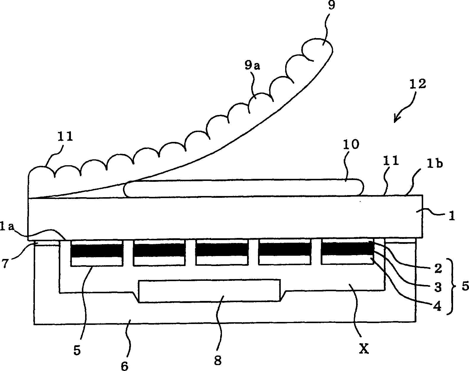
[0045] Figure 4 It is an explanatory view of the structure represented by the cross-section of Example 2 of the present invention. In this second embodiment, in the light-emitting display panel 12 of the first embodiment, instead of bonding the microlens array 9 to the other surface (upper surface) 1b of the transparent substrate 1 through the adhesive 10, the adhesive 10 The substrate 13 on which the microlens array 9 is disposed on one surface (upper surface) formed of the same material as the transparent substrate 1 is bonded to the other surface (upper surface) 1b of the transparent substrate 1 .
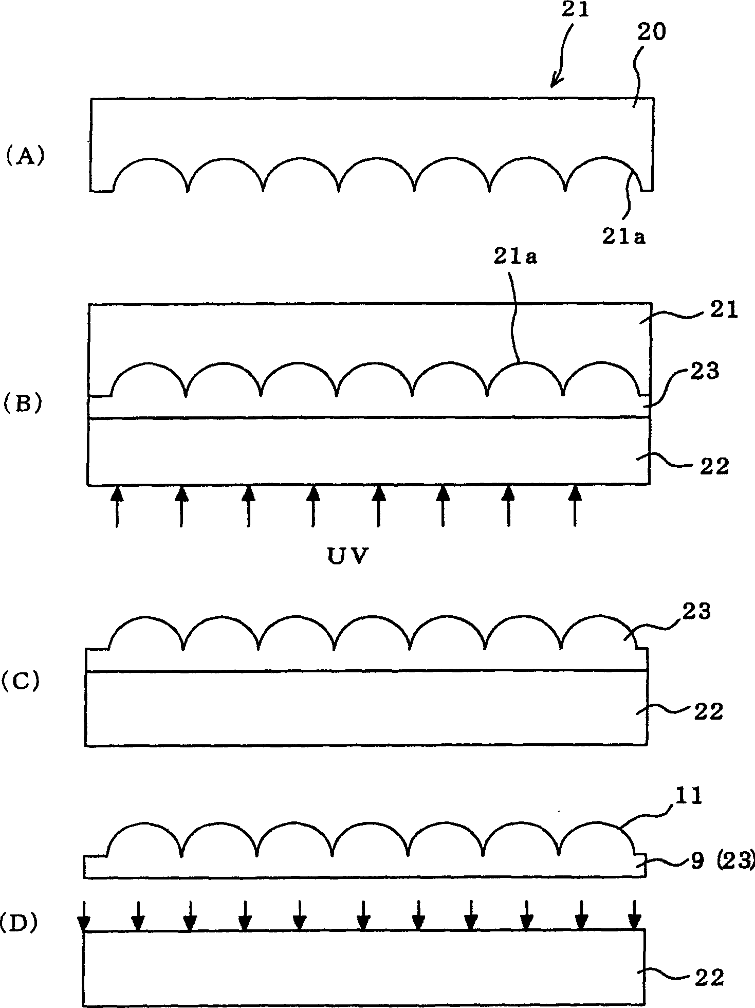
[0046] Here, using Figure 5 The process diagram of FIG. 1 illustrates the manufacturing process of the microlens array 9 .
[0047] (A) First, polysilicon is applied to the outer surface of the quartz glass plate 20 that is the model of the microlens array 9, and a hole is provided on one side (lower surface) at the position where the convex lens 9 is formed, and wet etching...
Embodiment 3
[0053] Embodiment 3 of the present invention, in the light-emitting display panel 12 of Embodiment 2, instead of bonding the substrate 13 configured with the microlens array 9 to the transparent substrate 1 through the adhesive 10, The substrate 14 on which the microlens array 9 is formed is bonded to the transparent substrate 1 .
[0054] Here, using Figure 6 The process diagram of FIG. 1 illustrates the manufacturing process of the microlens array 9 .
[0055] (A) First, the photosensitive resin 24 is applied to one surface (upper surface) 13a of the substrate 13 formed of the same material as the transparent substrate 1, in order to form corresponding microlenses for each light emitting element 5 (pixel). In the portion of the convex lens 9a of the array 9, the photosensitive resin 24 is image-overlaid by photolithography.
[0056] (B) Next, heat is applied to the photosensitive resin 24 on which the image has been superimposed, and the surface is rounded (heat reflowed)...
PUM
 Abstract
Description
Claims
Application Information