Optical module and manufacturing method of the same, optical communication device, photoelectric hybrid integrated circuit, circuit board, electronic device

A technology of optical modules and paths, applied in the coupling of optical waveguides, installation of optical fibers/cables, optics, etc., can solve problems such as damage to the light-emitting surface and attachment of foreign objects

Inactive Publication Date: 2004-08-25
SEIKO EPSON CORP
View PDF1 Cites 39 Cited by
  • Summary
  • Abstract
  • Description
  • Claims
  • Application Information

AI Technical Summary

Problems solved by technology

Therefore, when the small connector is unplugged, the light-emitting / light-receiving surface of the optical element and the end surface of the optical fiber are exposed, and problems such as damage to the light-emitting surface or adhesion of foreign objects are likely to occur.

Method used


Image

  • Optical module and manufacturing method of the same, optical communication device, photoelectric hybrid integrated circuit, circuit board, electronic device
  • Optical module and manufacturing method of the same, optical communication device, photoelectric hybrid integrated circuit, circuit board, electronic device
  • Optical module and manufacturing method of the same, optical communication device, photoelectric hybrid integrated circuit, circuit board, electronic device

Examples


no. 2 Embodiment

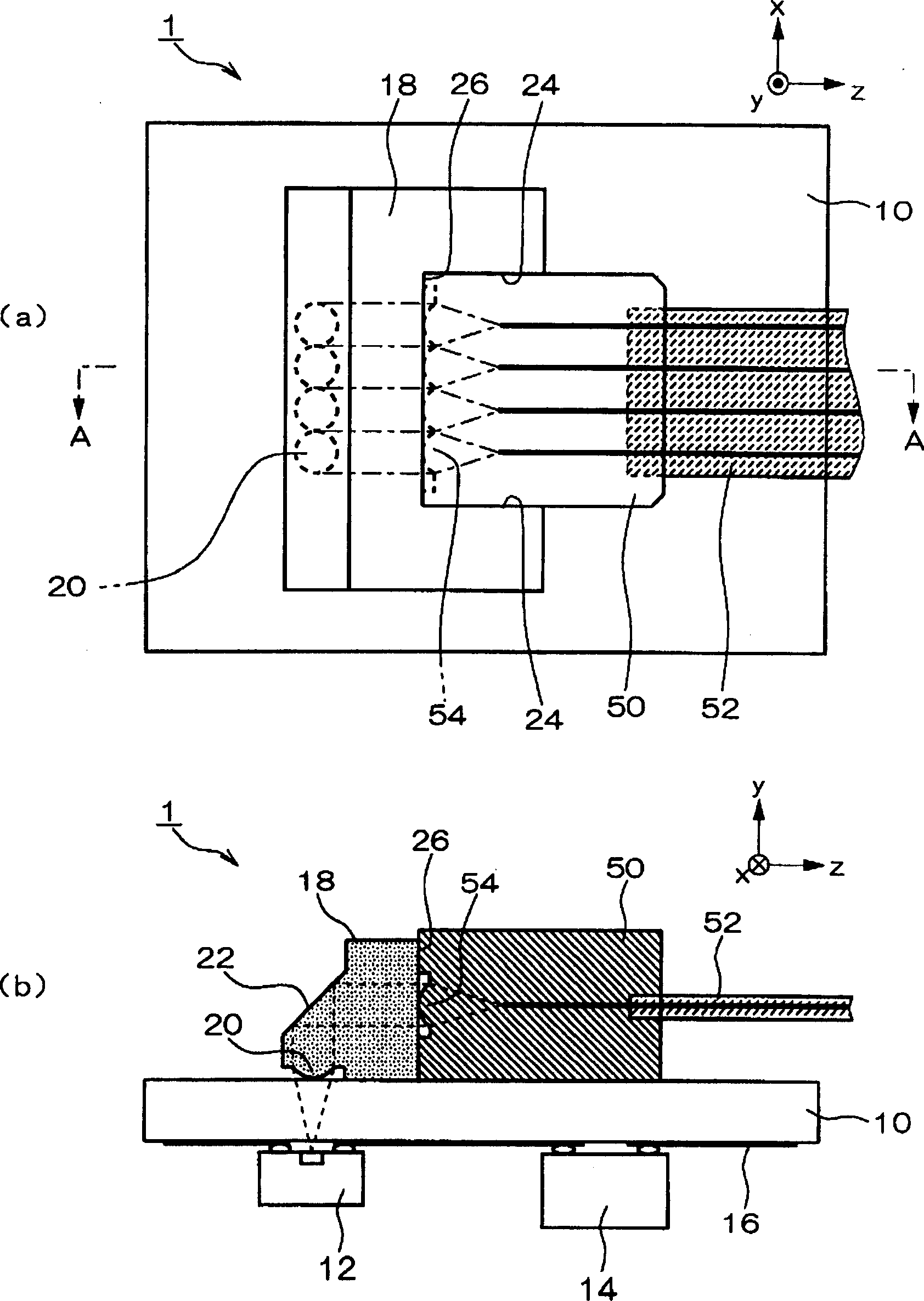
[0069] Figure 5 is a schematic diagram of the configuration of the optical module of the second embodiment. Figure 5 (a) is a plan view of the optical module of the present embodiment, Figure 5 (b) is along Figure 5 A cross-sectional view taken along line B-B in (a). The optical module 1a shown in this figure has basically the same configuration as the optical module 1 of the first embodiment, and common constituent elements are denoted by the same reference numerals. Hereinafter, differences will be mainly described.

[0070] Such as Figure 5 The optical module 1a shown differs from the first embodiment in the shape of the optical receptacle 18a to which the optical plug 50 is mounted. The optical receptacle 18a of this embodiment includes the surface 24 and the surface 26 as the guide surfaces similarly to the optical receptacle 18 described above, and also includes the surface 32 for determining the position of the optical module 1a in the y-axis direction. This ...

no. 3 Embodiment

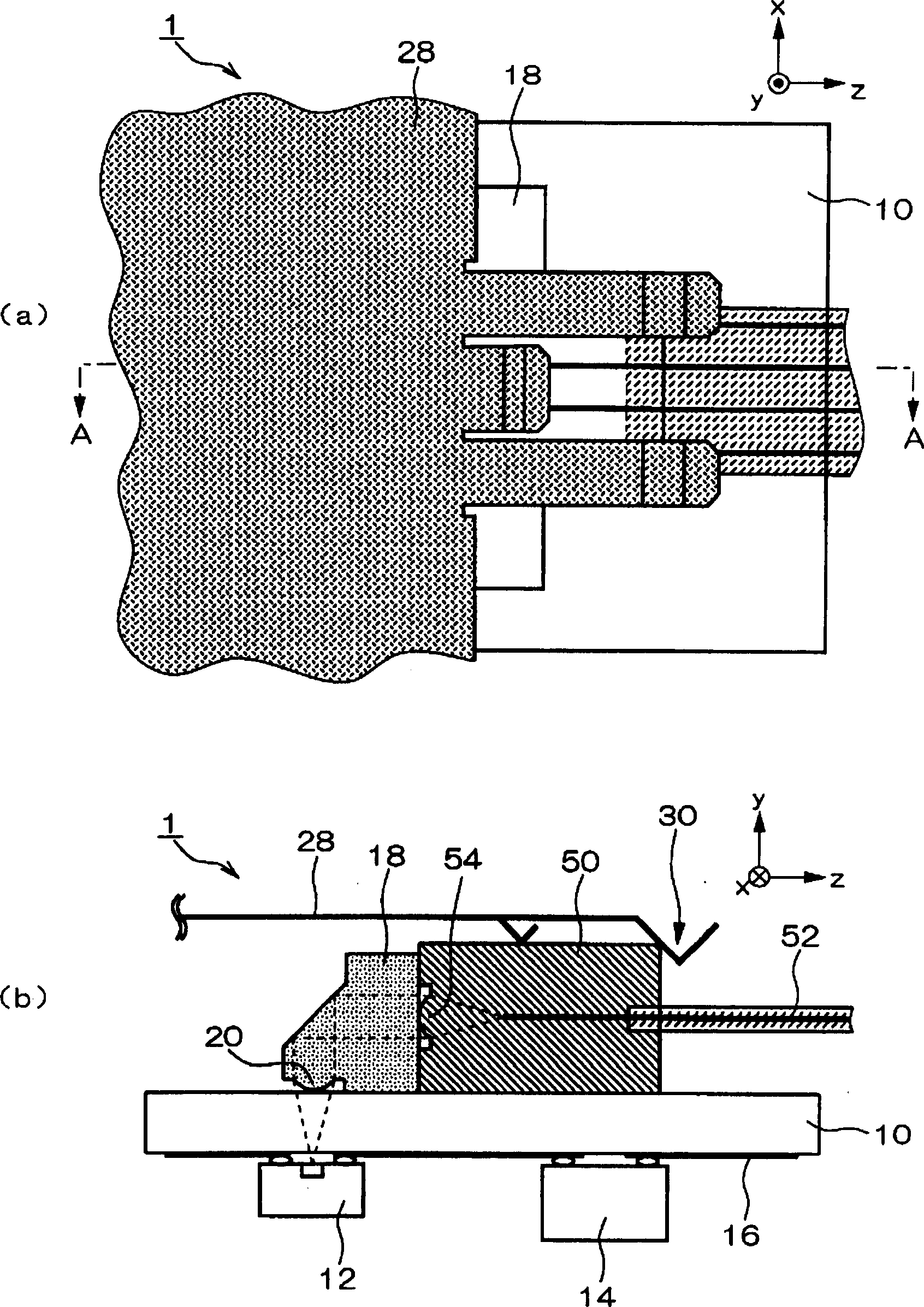
[0073] Figure 6 is a schematic diagram of the configuration of the optical module of the third embodiment. Figure 6 (a) is a plan view of the optical module of the present embodiment, Figure 6 (b) is along Figure 6 A cross-sectional view taken along line C-C in (a). The optical module 1b shown in this figure has basically the same configuration as the optical modules of the above-mentioned embodiments, and the common constituent elements are denoted by the same symbols. Hereinafter, differences will be mainly described.

[0074] Such as Figure 6 In the shown optical module 1b, the shape of the optical receptacle 18b for mounting the optical plug 50 is different from that of the above-mentioned embodiments. The optical receptacle 18b of this embodiment includes the surface 24a, the surface 26a, and the surface 32a as guide surfaces similarly to the above-mentioned optical receptacle 18a. The functions of the surface 24a, the surface 26a, and the surface 32a are the s...

no. 4 Embodiment

[0077] Figure 7 is a schematic diagram of the configuration of the optical module of the fourth embodiment. Figure 7 (a) is a plan view of the optical module of the present embodiment, Figure 7 (b) is along Figure 7 A cross-sectional view taken along line D-D in (a). The optical module 1c shown in this figure has the same configuration as the optical module of each of the above-mentioned embodiments, and common constituent elements are denoted by the same reference numerals. Hereinafter, differences will be mainly described.

[0078] Such as Figure 7 The illustrated optical module 1c has a configuration in which an optical plug 50b and an optical receptacle 18c can be directly mounted. Specifically, the optical receptacle 18c includes a surface 26b as a guide surface, and the optical connector 50b is mounted by adhering the surface 26b and the bonding surface provided on the optical connector 50b.

[0079] Furthermore, in this example, the lens 54b as the second len...


PUM


Abstract

Described is an optical module (1) capable of miniaturization, to which an optical plug (50) provided at one end of an optical transmission path (52) can be attached, so as to transmit and receive signal light via the optical transmission path (52) for information communication. The optical module (1) comprises: a transparent substrate (10) having light transmittance property with respect to the wavelength of used signal light; an optical socket (18), which is arranged on one surface side of the transparent substrate and to which the optical plug (50) can be attached; an optical element (12), which is arranged on the other surface side of the transparent substrate (10) and emits the signal light to the one surface side of the transparent substrate (10) according to a supplied electrical signal, or generates an electrical signal according to the intensity of the signal light supplied from the other surface of the transparent substrate (10); and a reflective portion (22), which is arranged on the other surface of the transparent substrate (10) and changes a path of the signal light emitted from the optical element (12) at substantially 90 degrees to guide it to the optical transmission path (52), or changes a path of the signal light emitted from the optical transmission path (52) at substantially 90 degrees to guide it to the optical element (12).

Description

technical field [0001] The present invention relates to devices, components, etc. used when performing information communication (signal transmission) between a plurality of devices or within a device using optical signals. Background technique [0002] In recent years, with the rapid development of signal transmission speed between circuit chips or circuit boards in various devices, crosstalk interference between signal lines, noise radiation, impedance mismatch, high power consumption, etc. have become problems that cannot be ignored . As a result, even the signal transmission inside the device begins to use optical communication. Instead of the existing method of using metal wiring to transmit electrical signals between circuit chips or modules in the device, optical transmission paths such as optical fibers (with optical fibers) and optical waveguides are used. The technology of communicating by optical signals is being widely used. Such a technology is described in th...

Claims


Application Information

Patent Timeline
Patent Type & Authority Applications(China)
IPC IPC(8): G02B6/38G02B6/42
CPCG02B6/4249G02B6/4292G02B6/4214G02B6/3845G02B6/3839
Inventor 长坂公夫金子丈夫宫前章
Owner SEIKO EPSON CORP
Why Eureka
Try Eureka