Apparatus for testing semiconductor integrated circuit

A technology of integrated circuits and testing devices, applied in the field of testing devices of semiconductor integrated circuits, can solve problems such as insufficient test functions to be further expanded

Inactive Publication Date: 2004-09-01
RENESAS TECH CORP
View PDF3 Cites 13 Cited by
  • Summary
  • Abstract
  • Description
  • Claims
  • Application Information

AI Technical Summary

Problems solved by technology

However, even the test machine of this previous application is not enough to further expand its testing capabilities

Method used


Image

  • Apparatus for testing semiconductor integrated circuit
  • Apparatus for testing semiconductor integrated circuit
  • Apparatus for testing semiconductor integrated circuit

Examples


Embodiment 1

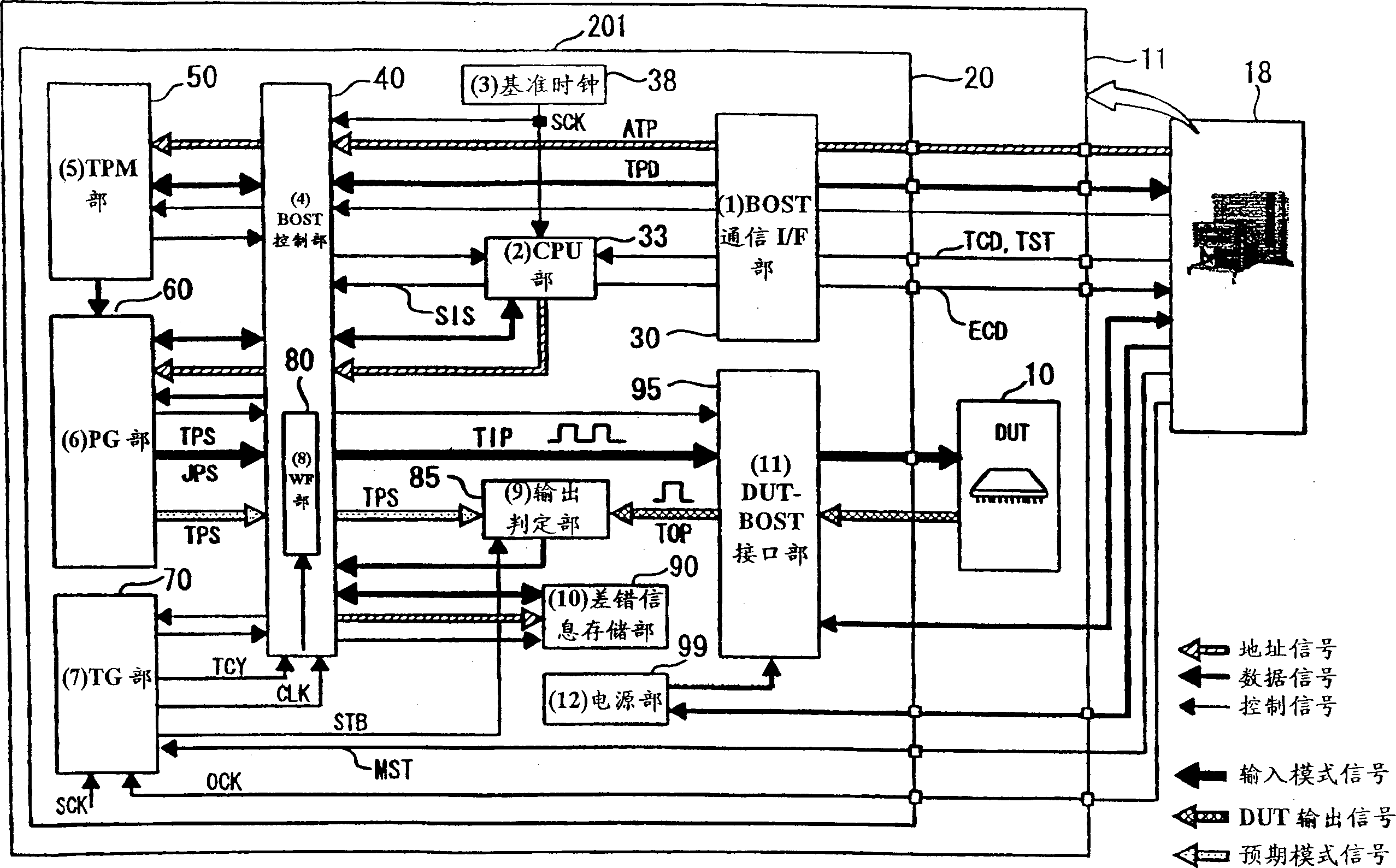
[0051] figure 1 It is a block diagram showing the circuit configuration of Embodiment 1 of the test device for semiconductor integrated circuits of the present invention. FIG. 2 is a block diagram showing the circuit configuration of the test support device of the first embodiment. FIG. 3 is a timing chart showing the test operation of Embodiment 1. FIG. In the test process of the method of manufacturing a semiconductor integrated circuit of the present invention, the test device of the first embodiment is used.

[0052] First, refer to figure 1 The overall circuit configuration of Embodiment 1 will be described. The test device for a semiconductor integrated circuit of the first embodiment is a test device for a semiconductor integrated circuit 10 to be tested, and includes a test circuit board 11 , an external tester 18 and a test auxiliary device 20 . The semiconductor integrated circuit 10 under test may also be called a DUT (Device Under Test). Various types of LSI c...

Embodiment 2-1

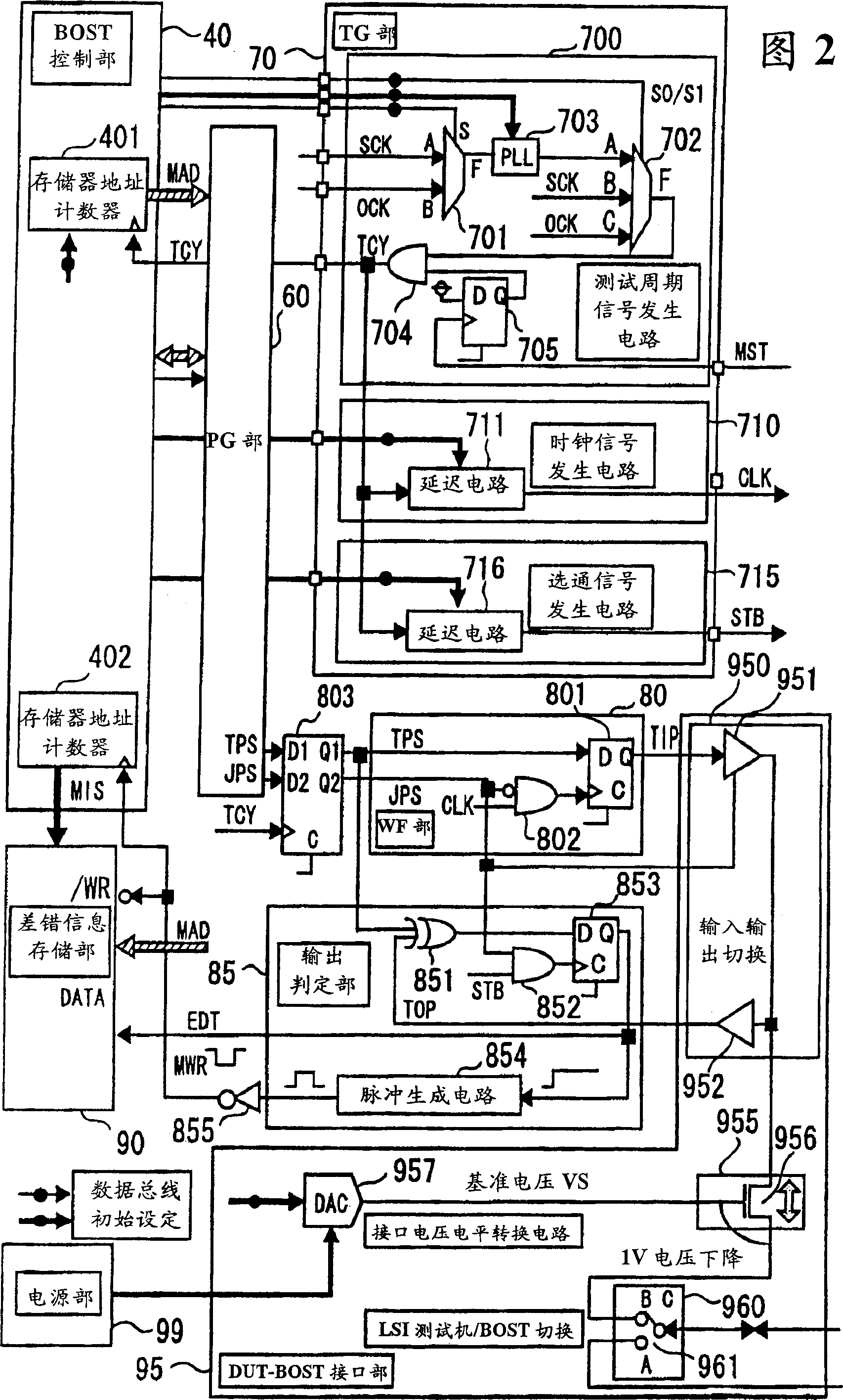
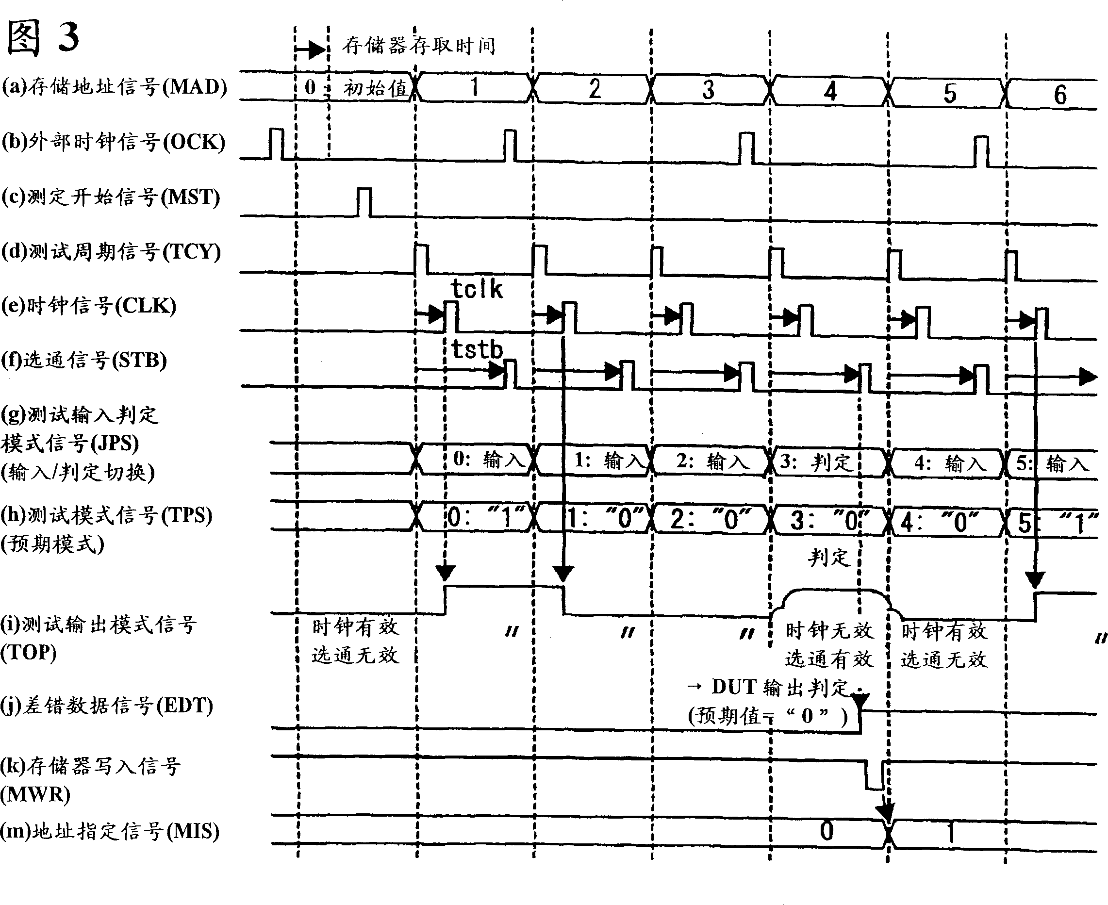
[0124] The present embodiment 2-1 is an embodiment of the semiconductor integrated circuit testing device of the present invention capable of commanding and controlling the test vectors of the test mode signal TPS. Shown in Fig. 4 the hardware structure of present embodiment 2-1, and use Figure 5 to Figure 8 The timing diagram represents the test operation according to the structure.

[0125] First, the hardware configuration of the present embodiment 2-1 will be described with reference to FIG. 4 . Fig. 4 (a) shows the structure of the BOST control unit 40 of the present embodiment 2-1, Fig. 4 (b) shows the memory structure of the PG part 60 corresponding to the present embodiment 2-1, and Fig. 4 (c) shows the diagram in detail The pulse generating circuit 417 shown in 4(a).

[0126] In this embodiment 2-1, figure 1The PG section 60 of the BOST device 20 shown in has the memory structure shown in FIG. 4( b ). The PG portion 60 is provided with a storage area 614 storing ...

Embodiment 2-2

[0180] The present embodiment 2-2 relates to the test device of the semiconductor integrated circuit of the present invention which is suitable for testing the digital circuits arranged in a matrix, such as a semiconductor memory, especially in the present embodiment 2-2, the PG part 60 has a Controls the ability to generate algorithmic test patterns. 9, 32, and 33 show the structures of the BOST control section 40 and the PG section 60 of the present embodiment 2-2, Figure 12 , Figure 14 , Figure 16 and Figure 18 An operation timing chart of the present embodiment 2-2 is shown.

[0181] In the semiconductor memory as the DUT 10 , a plurality of X-direction lines and a plurality of Y-direction lines are arranged in a matrix form perpendicular to each other, and memory cells are respectively located at their respective intersections. Multiple X-direction lines are selected by the X decoder, and multiple Y-direction lines are selected by the Y decoder. On the memory cel...


PUM


Abstract

An apparatus for testing a semiconductor integrated circuit has a test circuit board and an ancillary test device. The ancillary test device can test a digital circuit. The ancillary test device has test pattern memory, a test pattern signal generator, and a control section for controlling an operation for the test pattern data selected from among the plurality of test pattern data sets stored in the test pattern memory and an operation for writing the selected test pattern data into the test pattern signal generator. The ancillary test device generates a test input pattern signal on the basis of test pattern data written in the test pattern signal generator and determines a test output pattern signal output from the semiconductor integrated circuit on the basis of the test input pattern signal, thereby testing a digital circuit.

Description

technical field [0001] The present invention relates to a test device for a semiconductor integrated circuit in which a test auxiliary device is provided near a test circuit board for exchanging signals with a semiconductor integrated circuit to be tested, and a method for manufacturing a semiconductor integrated circuit using the device. Background technique [0002] In general, testing of a simulated large scale semiconductor integrated circuit (hereinafter referred to as LSI) is performed by using a dedicated tester for simulation. The structure of the simulation dedicated testing machine is designed to: provide test input signals to the DUT through a test circuit board that exchanges signals with the semiconductor integrated circuit under test (hereinafter referred to as DUT), and receive test output signals from the DUT for analysis. However, in recent semiconductor integrated circuits, there are increasing numbers of LSIs in which digital circuits are added to analog L...

Claims


Application Information

Patent Timeline
Patent Type & Authority Applications(China)
IPC IPC(8): G01R31/3183G01R31/28G01R31/316G01R31/319G06F11/263G11C29/56
CPCG01R31/31905G01R31/31926G06F11/263G11C29/56G01R31/31919
Inventor 森长也船仓辉彦花井寿佳
Owner RENESAS TECH CORP
Why Eureka
Try Eureka