
Deflector, method of manufacturing deflector, and charged particle beam exposure apparatus using deflector

A technology of charged particle beam and manufacturing method, which is applied in the direction of photolithographic exposure device, electric recording process using charge pattern, equipment for electric recording process using charge pattern, etc., which can solve processing line pollution, pollution, and difficult blanking Electrode and other problems, to achieve the effect of solving pollution problems, preventing falling off and deformation, and preventing charging

Inactive Publication Date: 2004-09-01
CANON KK +1
View PDF0 Cites 12 Cited by
  • Summary
  • Abstract
  • Description
  • Claims
  • Application Information

AI Technical Summary

Problems solved by technology

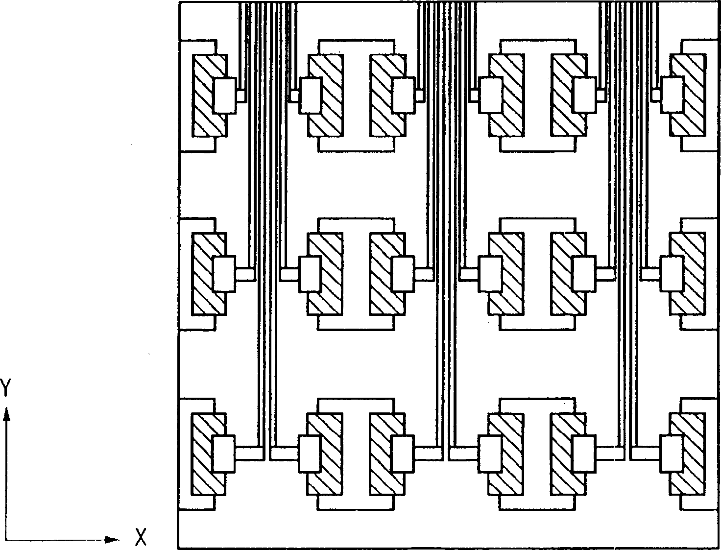
as from image 3 As can be seen, in the wiring removal direction ( image 3 In the case of Y direction), as the number of wiring increases away from the center of the device, it is difficult to blank to thousands of units when the pitch between blankers is kept constant (for example: 100μm) Issues such as electrode wiring
[0007] In addition, there is also the issue of pollution in the processing line
Since many wirings are arranged on the blanking electrodes, the wiring design rule becomes sub- The unit of micron requires a processing device of a semiconductor LSI production line, but in the semiconductor processing line, in order to avoid heavy metal contamination, it is impossible to put the above-mentioned MEMS substrate produced by the MEMS processing line into the semiconductor processing line. Issues arising from constraints

Method used


Image

  • Deflector, method of manufacturing deflector, and charged particle beam exposure apparatus using deflector
  • Deflector, method of manufacturing deflector, and charged particle beam exposure apparatus using deflector
  • Deflector, method of manufacturing deflector, and charged particle beam exposure apparatus using deflector

Examples


Embodiment Construction

[0111]

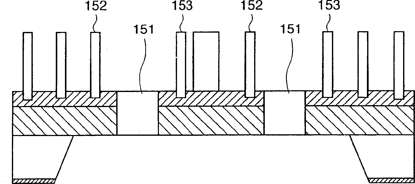
[0112] we refer to Figure 4A ~ Figure 10 A first embodiment of the deflector according to the present invention will be described on the side of the drawing. Figure 4A A plan view showing an electrode substrate 400 configured with blanking electrodes of a 3×3 blanker array, Figure 4B is a view of the electrode substrate 400 viewed from a cross-sectional direction (the insulator for insulating the blanking electrode and the electrode substrate is not shown). exist Figure 4A Among them, 52 and 53 are blanking electrodes, and 51 is an electron beam aperture. Figure 5 It is a plan view of the wiring substrate 500. 52P and 53P represent voltage-applying pads for applying voltage from an external power source (not shown in the figure), and 52' and 53' are for applying voltage from the pads 52P, 53P, and The wirings 52H and 53H of 53P are connection wiring pads for electrically connecting the electrodes 52 and 53 of the electrode substrate 400 . 51' is the electro...


PUM

PropertyMeasurementUnit
thicknessaaaaaaaaaa
thicknessaaaaaaaaaa
thicknessaaaaaaaaaa

Abstract

A deflector which makes multilayered wiring possible and prevents contamination during the manufacture includes an electrode substrate (400) having a plurality of through holes, and an electrode pair made up of first and second electrodes which oppose the side walls of each through hole in order to control the locus of a charged particle beam passing through the through hole, and a wiring substrate (500) having connection wiring pads connected to the electrode pairs of the electrode substrate to individually apply voltages to the electrode pairs. This deflector is formed by bonding the electrode substrate and wiring substrate via the connection wiring pads of the wiring substrate.

Description

technical field [0001] The present invention mainly relates to techniques applicable to charged particle beam exposure devices such as electron beam exposure devices and ion beam exposure devices used for exposure of semiconductor integrated circuits, and in particular, relates to pattern drawing using a plurality of charged particle beams. The deflection technology that can be applied in the charged particle beam exposure device and the charged particle beam exposure device using the deflection technology, etc. Background technique [0002] In the production of semiconductor devices, electron beam lithography technology is attracting attention as a powerful technology for etching that can perform fine pattern exposure of 0.1 μm or less. There are several methods for this etching, but there are problems to be solved in each method. For example, there is a so-called "variable rectangular beam method" that can draw a pattern with one stroke. However, the variable rectangular...

Claims


Application Information

Patent Timeline
Patent Type & Authority Applications(China)
IPC IPC(8): G03F7/20H01J37/04H01J37/147H01J37/305H01J37/317H01L21/027
CPCH01J2237/0435H01J37/3177B82Y10/00H01J37/045B82Y40/00H01J2237/0437
Inventor 小野治人赤池正刚玉森研尔广濑太小山泰史寺崎敦则长永兼一中山义则
Owner CANON KK
Learn More