Planar display with non-matrix shading structure
一种平面显示器、遮光结构的技术,应用在非线性光学、静态指示器、光学等方向
- Summary
- Abstract
- Description
- Claims
- Application Information
AI Technical Summary
Problems solved by technology
Method used
Image

Examples
no. 1 example
[0092] In the first embodiment, a transmissive liquid crystal display is taken as an example, and a TFT is used as a driving element.
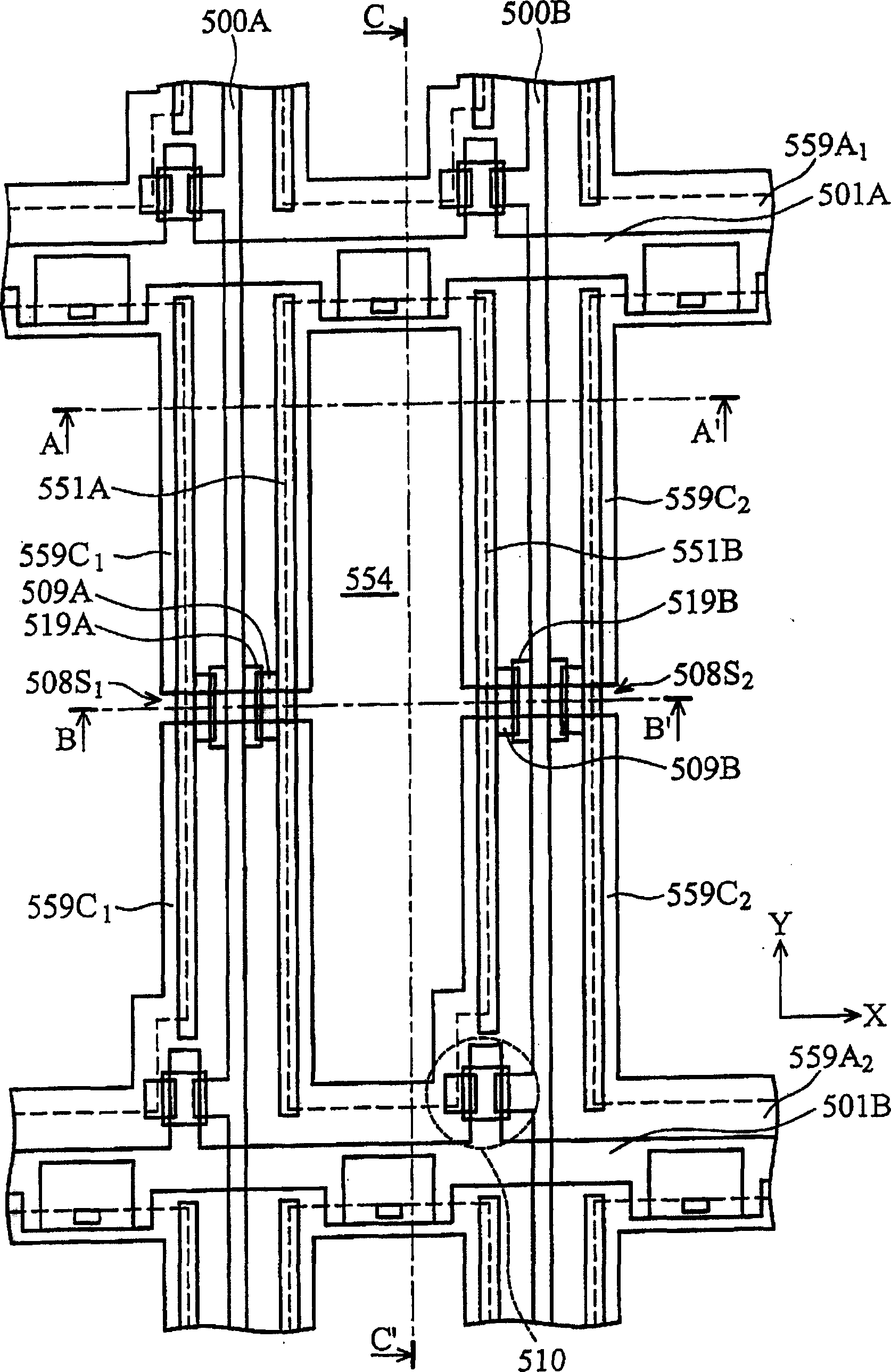
[0093] figure 1 is a plan view of a pixel area of the liquid crystal display in the first embodiment of the present invention. Figure 2A , Figure 2B with Figure 2C respectively figure 1 Sectional views of the A-A', B-B' and C-C' tangents of . Figure 5 yes figure 1 The plan view of the main light-shielding structure in the pixel area of , the light-shielding structure is arranged on the upper transparent substrate.
[0094] image 3 is a plan view of a fishbone-shaped shading element located on an upper transparent substrate in a plurality of adjacent pixel areas, Figure 4 is a plan view of the herringbone space between the herringbone-shaped shading elements in multiple adjacent pixel areas.
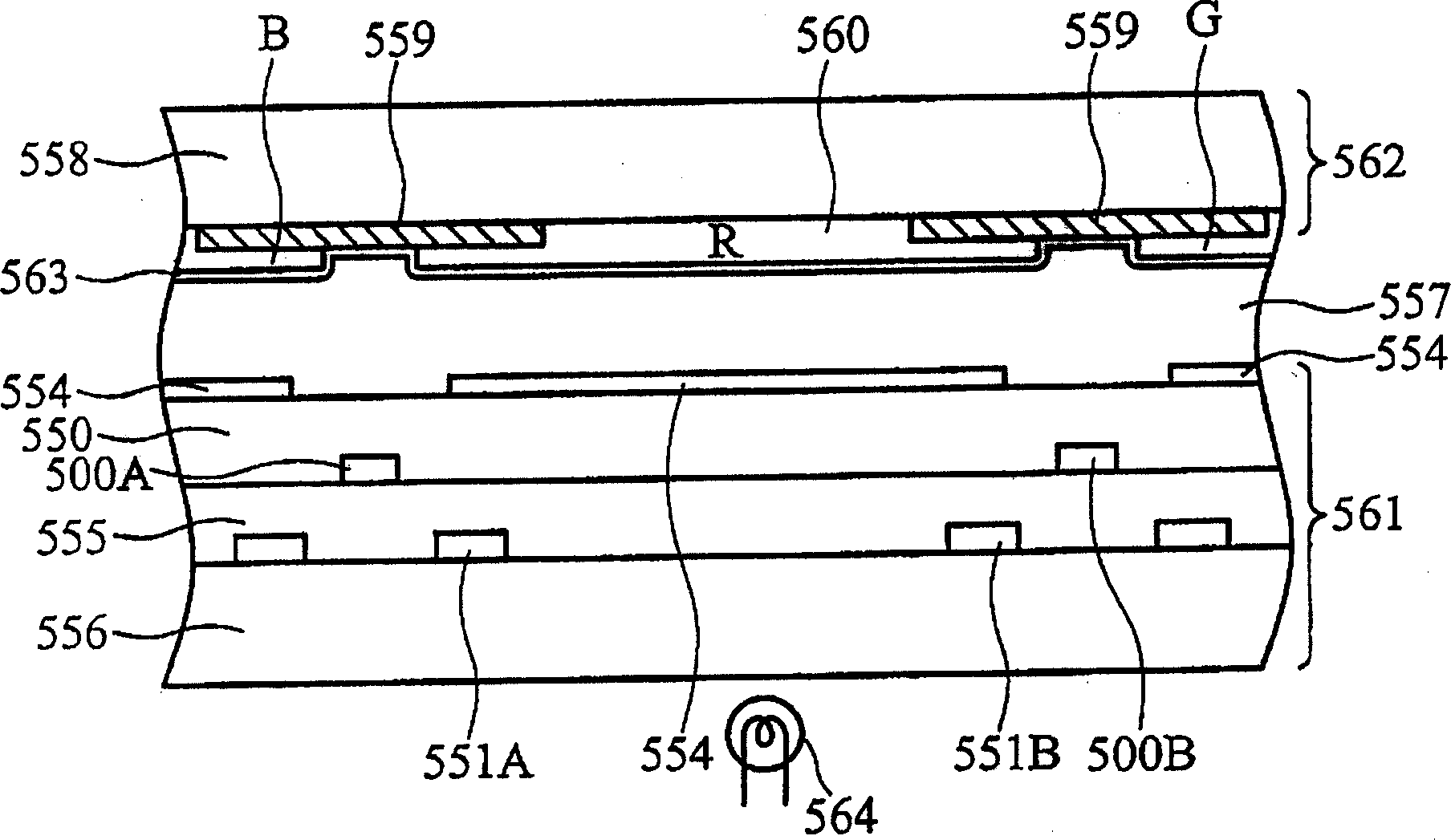
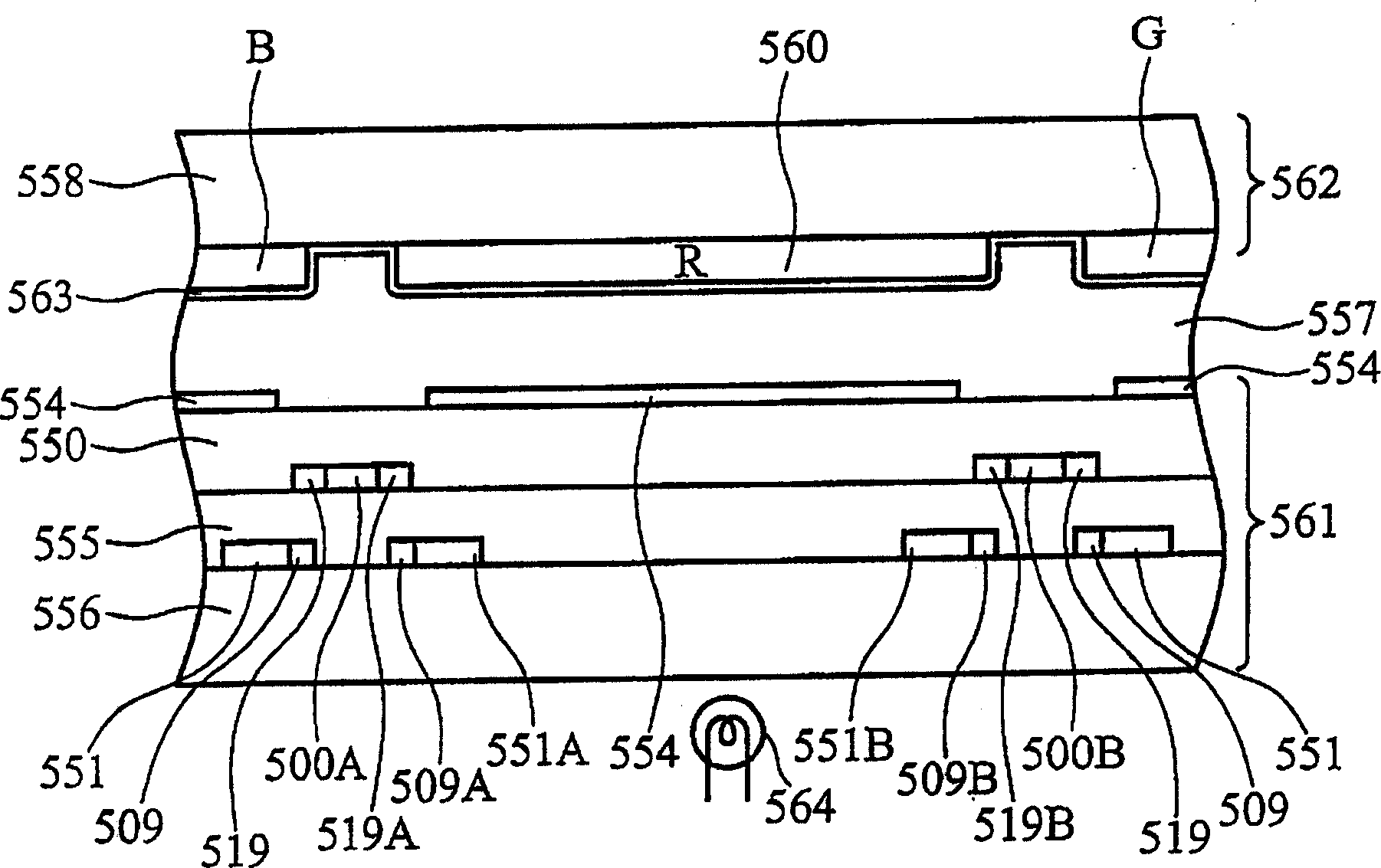
[0095] Such as Figure 2A to Figure 2C As shown, the liquid crystal display includes an upper substrate 562, a lower substrate 561,...
no. 2 example
[0107] In the second embodiment, a transmissive liquid crystal display is taken as an example, and a TFT is used as a driving element.
[0108] Figure 11 is a plan view of a pixel region of a liquid crystal display according to a second embodiment of the present invention. Figure 12A , Figure 12B with Figure 12C are respectively Figure 11 Sectional views of the A-A', B-B' and C-C' tangents of . Figure 14 yes Figure 11 A plan view of two adjacent herringbone-shaped shading elements disposed on the upper transparent substrate in the pixel area of .
[0109] Figure 13 is a plan view of fishbone-shaped shading elements in a plurality of adjacent pixel areas, Figure 15 It is a structural configuration diagram of a multi-pixel area.
[0110] Such as Figure 12A to Figure 12C As shown, the liquid crystal display includes an upper substrate 662, a lower substrate 661, and a liquid crystal layer 657 interposed therebetween. The light source 664 is disposed behind t...
no. 3 example
[0123] Such as Figure 7 with Figure 15 As shown, the incident light passing through the gaps 508S and 608S in the main light-shielding structures 559 and 659 will be blocked by the auxiliary light-shielding structures in different layers. Space provided by gaps 508S and 608S can be used to avoid stress across the entire LCD panel.
[0124] refer to Figure 16 , in the third embodiment, the gaps 708S are randomly placed on the scan lines 701 and the signal lines 700 . Each main space 708L corresponding to the pixel electrode 754 (shown by a dotted line) is connected to at least one gap 708S disposed on the scan line 701 or the signal line 700 , and is connected to an adjacent main space 708L through the gap 708S.
[0125] If the gap 708S of the main light-shielding structure 759 is disposed on the scan line 701 and the capacitor 705 , the auxiliary light-shielding layer 739 disposed under the main light-shielding structure 759 and extending from the scan line 701 can block...
PUM
 Abstract
Description
Claims
Application Information
 - Generate Ideas
- Intellectual Property
- Life Sciences
- Materials
- Tech Scout
- Unparalleled Data Quality
- Higher Quality Content
- 60% Fewer Hallucinations
Browse by: Latest US Patents, China's latest patents, Technical Efficacy Thesaurus, Application Domain, Technology Topic, Popular Technical Reports.
© 2025 PatSnap. All rights reserved.Legal|Privacy policy|Modern Slavery Act Transparency Statement|Sitemap|About US| Contact US: help@patsnap.com