Working table device, film-forming device, optical element, semiconductor element and electronic device

A film-forming device and workbench technology, which is applied in the direction of semiconductor devices, semiconductor/solid-state device manufacturing, metal processing equipment, etc., can solve problems such as difficulty in forming uniform layers, short circuits in circuit patterns, film formation or drying effects of light-emitting layers, etc.

Inactive Publication Date: 2004-10-13
SEIKO EPSON CORP
View PDF1 Cites 12 Cited by
  • Summary
  • Abstract
  • Description
  • Claims
  • Application Information

AI Technical Summary

Problems solved by technology

[0004] However, there may be cases where static eliminators do not have sufficient static removal capability
In addition, since the latter technology is aimed at holding relatively hard substrates such as semiconductor wafers, the hole diameters formed on the table device are relatively large. When the substrate, that is, the flexible substrate is adsorbed, it is easy to leave adsorption marks on the substrate
If the adsorption marks remain on the flexible substrate, it will have a great influence on the film formation or drying of the light-emitting layer, etc., making it difficult to form a uniform layer, resulting in uneven light emission or short-circuiting of circuit patterns.

Method used


Image

  • Working table device, film-forming device, optical element, semiconductor element and electronic device
  • Working table device, film-forming device, optical element, semiconductor element and electronic device
  • Working table device, film-forming device, optical element, semiconductor element and electronic device

Examples


Embodiment Construction

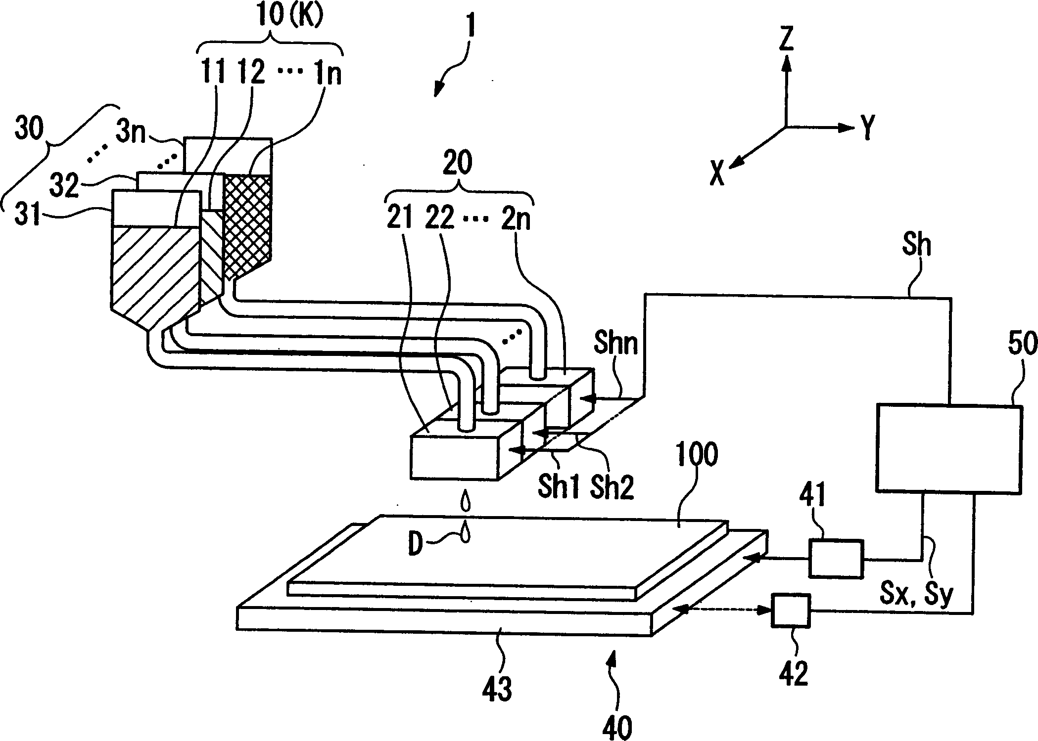
[0025] figure 1 It is a schematic diagram showing the film forming apparatus 1 of the present invention. The film forming apparatus 1 is an apparatus for forming a film by ejecting liquid droplets by an inkjet method, and includes an inkjet head 20 , a storage tank 30 , a stage device 40 , and a control device 50 .

[0026] In addition, the substrate 100 used in the present invention is a thin plastic or film-like flexible substrate, that is, a so-called flexible substrate, which is placed on the table device 40, and the liquid droplets ejected by the inkjet nozzle 20, etc. It lands thereon to form a film such as a light-emitting layer or a conductive layer.

[0027] Furthermore, as the material of the substrate 100 , transparent materials such as plastics such as polyolefin, polyester, polyacrylate, polycarbonate, polyethersulfone, and polyetherketone can be used.

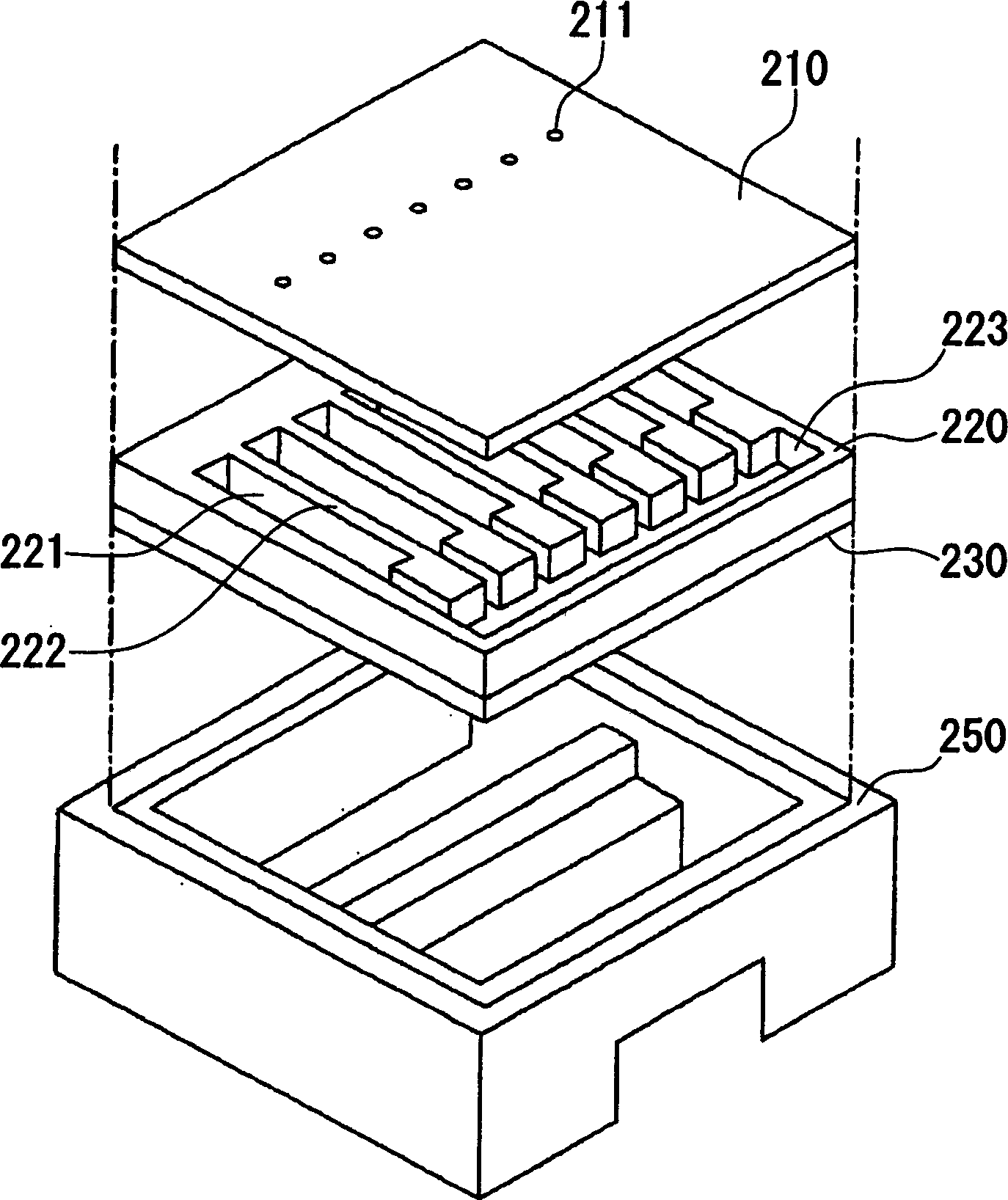
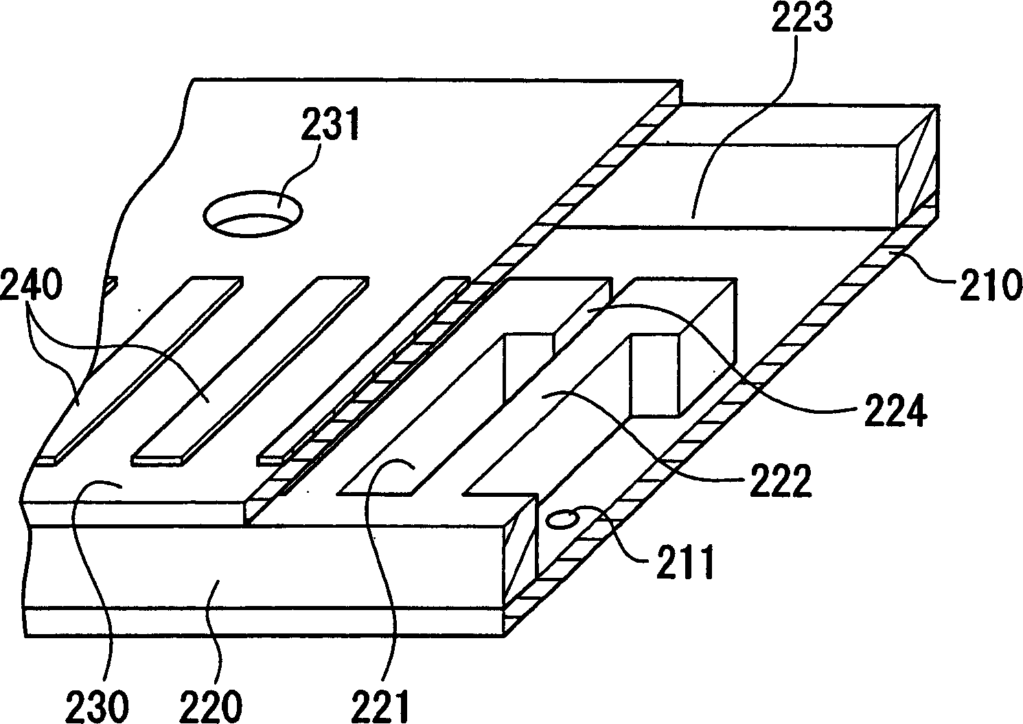
[0028] The inkjet heads 20 (21 to 2n: n is an arbitrary natural number) each have the same structure, and can...


PUM


Abstract

This table device 40 sucks and holds the substrate 100, and includes a sucking part 43 formed of a porous body. A conductive film 44 is formed on the substrate sucking surface in the sucking part, and the conductive film 44 is made to be grounded.

Description

technical field [0001] The present invention relates to an adsorption stage used in the manufacturing process of electronic equipment and the like to adsorb and hold a flexible substrate. Background technique [0002] Organic EL (Electroluminescence) elements, which can make display devices thinner than liquid crystal displays, are attracting attention as a next-generation technology. If organic EL elements are arranged on flexible plastic, it can also be made into a display device that is as thin as paper and can be bent. In addition, in the manufacture of organic EL (electroluminescent) display devices or TAB (Tape Automated Bonding), a technique is used in which a luminescent material, a conductive Droplets of materials, etc., form light-emitting layers or circuit patterns. At this time, in order to hold the substrate or the like on the stage device, the stage device is generally formed of a porous body, and the substrate is adsorbed and held by the pores formed in the ...

Claims


Application Information

Patent Timeline
Patent Type & Authority Applications(China)
IPC IPC(8): B23Q3/08B41J2/175H01L21/68H01L51/50H05B33/10H05B33/12
CPCB41J2/17509Y10T279/23H01L21/68
Inventor 渡边信子
Owner SEIKO EPSON CORP
Why Eureka
Try Eureka