Semiconductor storage device
A storage device and semiconductor technology, applied in semiconductor devices, information storage, semiconductor/solid-state device manufacturing, etc., can solve the problem of increasing the cost of aging devices, increasing the chip area of flash EEPROM devices 110, increasing the cost of testing chips for flash EEPROM devices, etc. question
- Summary
- Abstract
- Description
- Claims
- Application Information
AI Technical Summary
Problems solved by technology
Method used
Image
Examples
Embodiment 1
[0087] Embodiment 1 of the present invention will be described with reference to the drawings.
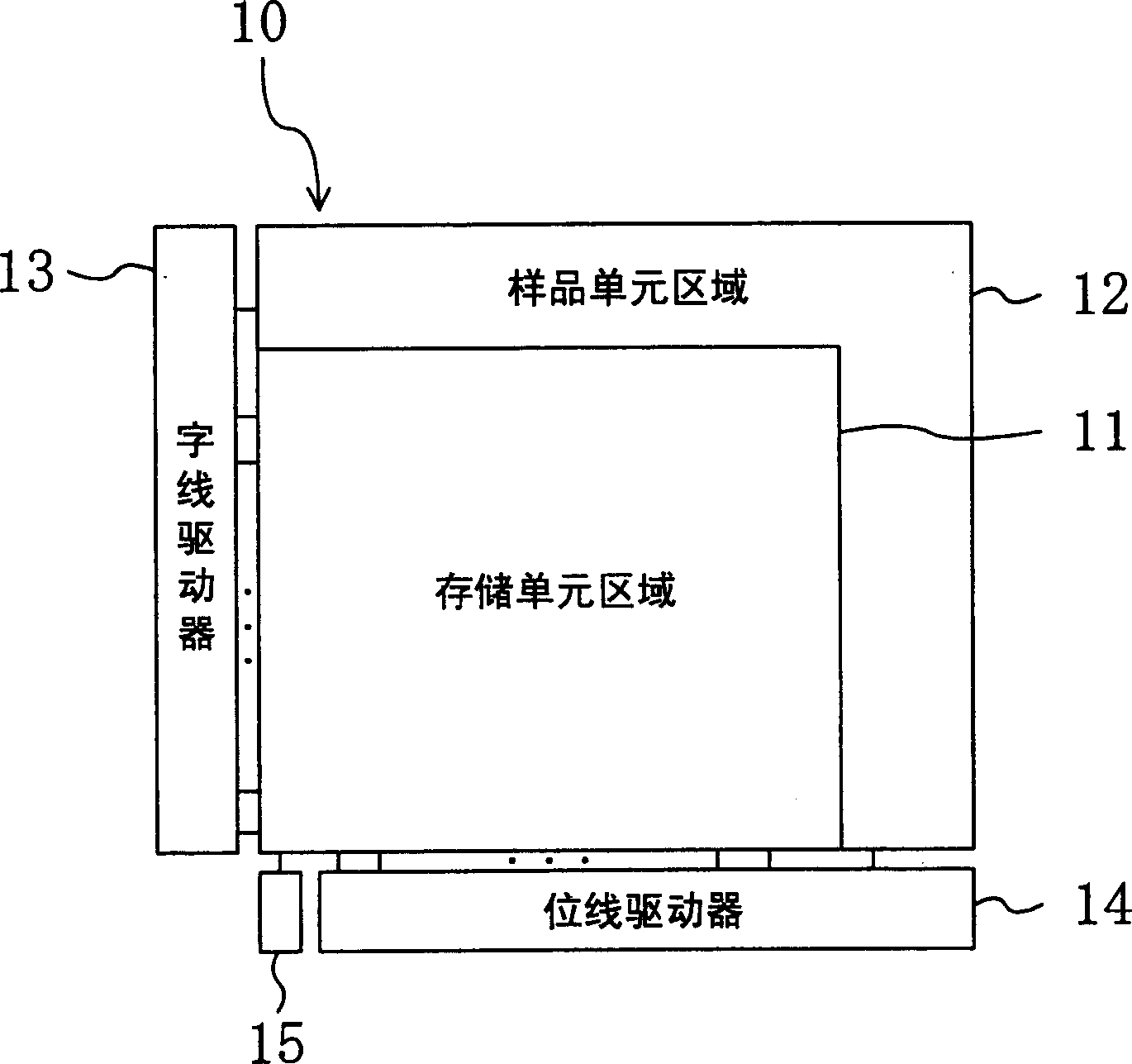
[0088] figure 1 A block diagram showing the configuration of the semiconductor memory device according to Embodiment 1 of the present invention. Such as figure 1 As shown, the semiconductor storage device of Embodiment 1 is equipped with a memory cell array 10 in which a plurality of memory cells are arranged in rows and columns. Apply a stress voltage to the sample region 12. Furthermore, as a peripheral circuit for driving the memory cell array 10, a word line driver 13 for driving the word line of the memory cell region 11 and the word line of the sample region 12 (hereinafter referred to as a sample word line) is provided; and a bit line driver 14 for the bit line of the sample region 12 (hereinafter referred to as a sample bit line); and a source line driver 15 for driving a common source line of the memory element region 11 and the sample region 12 .
[0089] Here, the ...
Embodiment 2
[0139] Hereinafter, a semiconductor memory device according to Embodiment 2 of the present invention will be described with reference to the drawings.
[0140] The configuration block diagram of the semiconductor memory device of Embodiment 2 and figure 1 Similarly, the difference from Embodiment 1 lies in that: in the memory cell array 10 , a switching device is provided to isolate the connection between the memory cell region 11 and the sample cell region 12 .
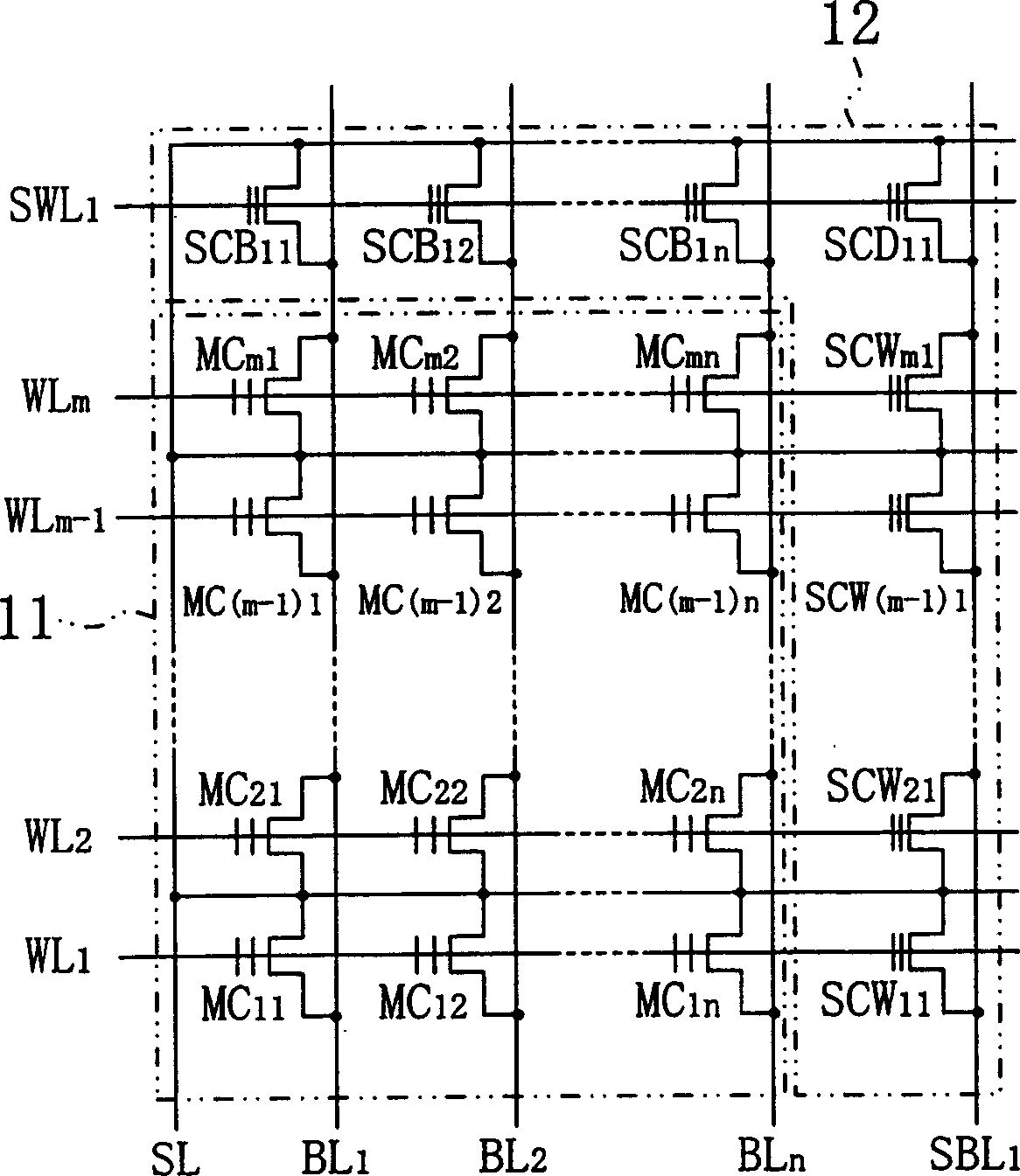
[0141] Figure 8 The circuit configuration of the memory cell array of the semiconductor memory device according to the second embodiment is shown. like Figure 8 As shown, in the memory cell array 10, as a switch device for controlling the connection between the memory cell region 11 and the sample cell region 12, sample cells SCW respectively connected to the word lines are provided. 11 ~SCW m1 with memory cell MC 1n ~MC mn The fuse FW between each control gate electrode 1 ~FW m , and set the sample cell S...
Embodiment 3
[0157] Hereinafter, a semiconductor memory device according to Embodiment 3 of the present invention will be described with reference to the drawings.
[0158] Figure 10 A block diagram showing the semiconductor memory device of the third embodiment. like Figure 10 As shown, averaging circuit 32 is provided on bit line driver 14 by intervening readout circuit 31 . In addition, the readout circuit 31 is a control circuit that performs a readout operation as described in the first embodiment.
[0159] The feature of the semiconductor storage device of Embodiment 3 is: in the sample cell region 12 of the memory cell array 10, a plurality of sample cells are respectively arranged on one bit line or one word line, and in the averaging circuit 32, a plurality of sample cells The amount of change in threshold voltage of the cells is averaged and read out.
[0160] Figure 11 It is a circuit diagram showing a memory cell array of the semiconductor memory device of the third emb...
PUM
 Abstract
Description
Claims
Application Information
 - R&D Engineer
- R&D Manager
- IP Professional
- Industry Leading Data Capabilities
- Powerful AI technology
- Patent DNA Extraction
Browse by: Latest US Patents, China's latest patents, Technical Efficacy Thesaurus, Application Domain, Technology Topic, Popular Technical Reports.
© 2024 PatSnap. All rights reserved.Legal|Privacy policy|Modern Slavery Act Transparency Statement|Sitemap|About US| Contact US: help@patsnap.com


