Exposure process for different levels

An exposure method and layered technology, applied in microlithography exposure equipment, photolithography exposure devices, optics, etc., can solve problems such as inapplicability, difficulty in evaluating the pros and cons of integrated circuits, and high manufacturing costs of photomasks

Inactive Publication Date: 2005-01-19
MACRONIX INT CO LTD
View PDF0 Cites 1 Cited by
  • Summary
  • Abstract
  • Description
  • Claims
  • Application Information

AI Technical Summary

Problems solved by technology

[0008] Due to mass production costs, most of the circuit images 11 on the mask 1 are designed to form the same integrated circuit layer, and these images 11 can be used at the same time to expose multiple places on the same chip to form potential images, so as to greatly reduce exposure costs time and save production cost; therefore, exposure forms a predetermined integrated circuit layer on the chip, that is, at least one mask must be used (if the complexity of the integrated circuit is considered, there are also multiple exposures to form a layer of integrated circuits using multiple masks), and When using one photomask, the photomask and the lithography machine must be positioned relative to each other once; in terms of the integration level of current components, a general chip must form at least six integrated circuit layers, that is to say, the photomask must be positioned relative to each other. At least six times with the lithography machine, and the accumulation of uncontrollable alignment errors will directly affect the chip integration and yield
[0009] Furthermore, due to the extremely high manufacturing cost of photomasks, chip foundries currently only carry out mass production. By mass producing chips with the same components, the cost of photomasks is shared to obtain commercial profits.
However, for design houses (design houses) that are generally not well-funded, the purpose of manufacturing components is generally to test the pros and cons of the integrated circuits they design, and to evaluate the feasibility of mass production and listing. Manufacturing chips is mainly based on small batches and diversity. Therefore, the current mass production method that must use a large number of photomasks is not applicable. It will affect the accuracy of its experimental production, and it is more difficult to evaluate the pros and cons of the integrated circuits it experiments

Method used


Image

  • Exposure process for different levels
  • Exposure process for different levels
  • Exposure process for different levels

Examples


Embodiment Construction

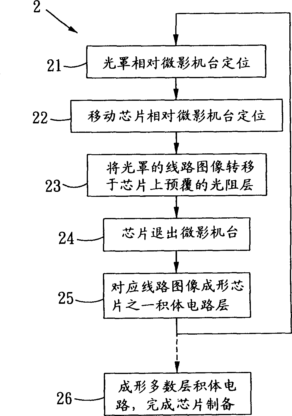
[0055] The different levels of exposure method 3 of the present invention is applicable to the manufacture of many chips in small batches, and a lithography machine is used to perform multi-level exposure on the chips. Each chip has a plurality of integrated circuit layers. In this example, a six-layer integrated circuit will be formed. layer as an example.

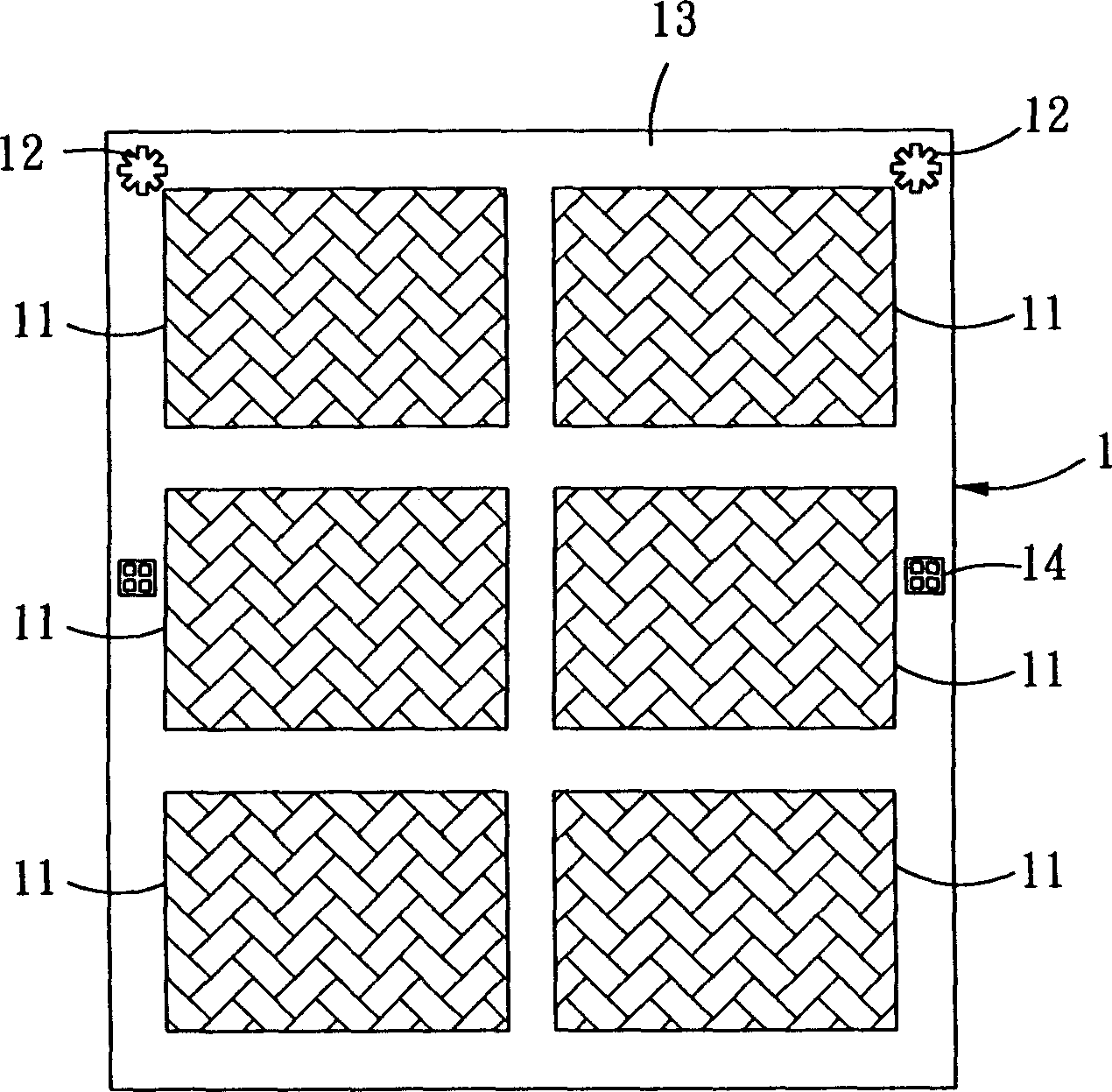
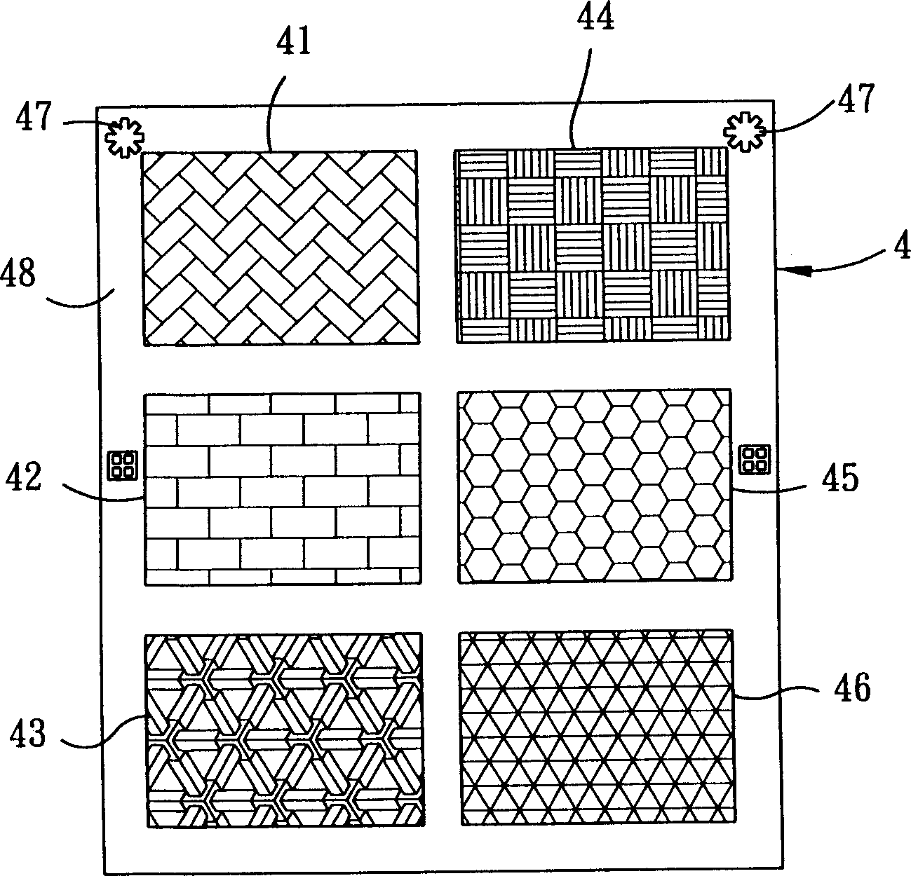
[0056] like image 3 As shown, the photomask 4 used in the present invention can be a binary photomask, or a phase shift photomask, including six different line images 41, 42, 43, 44, 45, 46, and most of them are located at the corners of the four corners. font or rice-shaped positioning mark 47 (in the icon, the rice-shaped character is used as an example), each of the circuit images 41, 42, 43, 44, 45, 46 is designed for each layer of integrated circuits, and these circuit images 41, 42, 43, 44, 45, 46 are also plated with a layer of chromium film with a thickness of about several hundred Å to form a non-light-transmit...


PUM


Abstract

It is a different-level exposure method to take multiple-level exposure to the chip with multiple integration circuit layers by a micro-image machine platform. The method are the following: A, to locate the light cover with multiple out-of-phase circuit images on the micro image machine platform; B, to locate the chip one the micro image machine platform; C, to form a integration circuit layer in the chip from a circuit image in the light cover; D, to re-locate the chip on the micro image machine and furthermore to form another integration circuit layer in the chip form the other circuit image in the cover. This invention adopts only one calibration mark on the cover to relevantly locate on the micro image machine, that is to selectively transfer the images separately on the pre-coat photoresist layer and to relevantly form at least one integration layer on the chip to lower the calibration errors of light cover.

Description

【Technical field】 [0001] The invention relates to an exposure method for an integrated circuit manufacturing process, in particular to a different-level exposure method capable of precisely positioning a photomask to reduce circuit image errors after exposure. 【Background technique】 [0002] Photolithography is one of the most important steps in the semiconductor manufacturing process. Anything related to the MOS structure, such as the pattern of each layer of thin film, doped regions (dopants), etc., is determined by this process. However, the technical level of the lithography process is generally not only determined by the number of masks required, but also because the more masks are used, the more times the masks need to be positioned, and the more likely it is to cause positioning corrections. Therefore, how to reduce the positioning error of positioning the mask to improve the alignment of the image is one of the industry's efforts to improve the yield of the lithograp...

Claims


Application Information

Patent Timeline
IPC IPC(8): G03F7/00G03F7/20H01L21/027
Inventor 林顺利杨金成吕文彬陈铭祥秦启元陈映仁
Owner MACRONIX INT CO LTD
Why Eureka
Try Eureka