Detecting device of printed circuit board for mounting electronic element and figure poorness identification method

A technology for electronic component installation and printed circuit board, which is applied to printed circuit components, electrical components, measuring devices, etc., can solve the problems of time-consuming and the number of bad detection positions, etc., and achieve the effect of efficient discrimination

Inactive Publication Date: 2005-02-02
MITSUI MINING & SMELTING CO LTD
View PDF3 Cites 6 Cited by
  • Summary
  • Abstract
  • Description
  • Claims
  • Application Information

AI Technical Summary

Problems solved by technology

[0007] In this way, for several defective detection positions detected in a part by the image processing device, ea

Method used


Image

  • Detecting device of printed circuit board for mounting electronic element and figure poorness identification method
  • Detecting device of printed circuit board for mounting electronic element and figure poorness identification method
  • Detecting device of printed circuit board for mounting electronic element and figure poorness identification method

Examples


Embodiment Construction

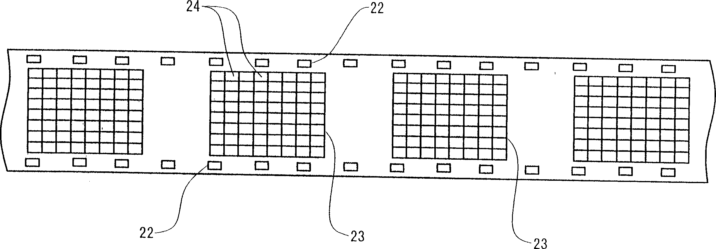
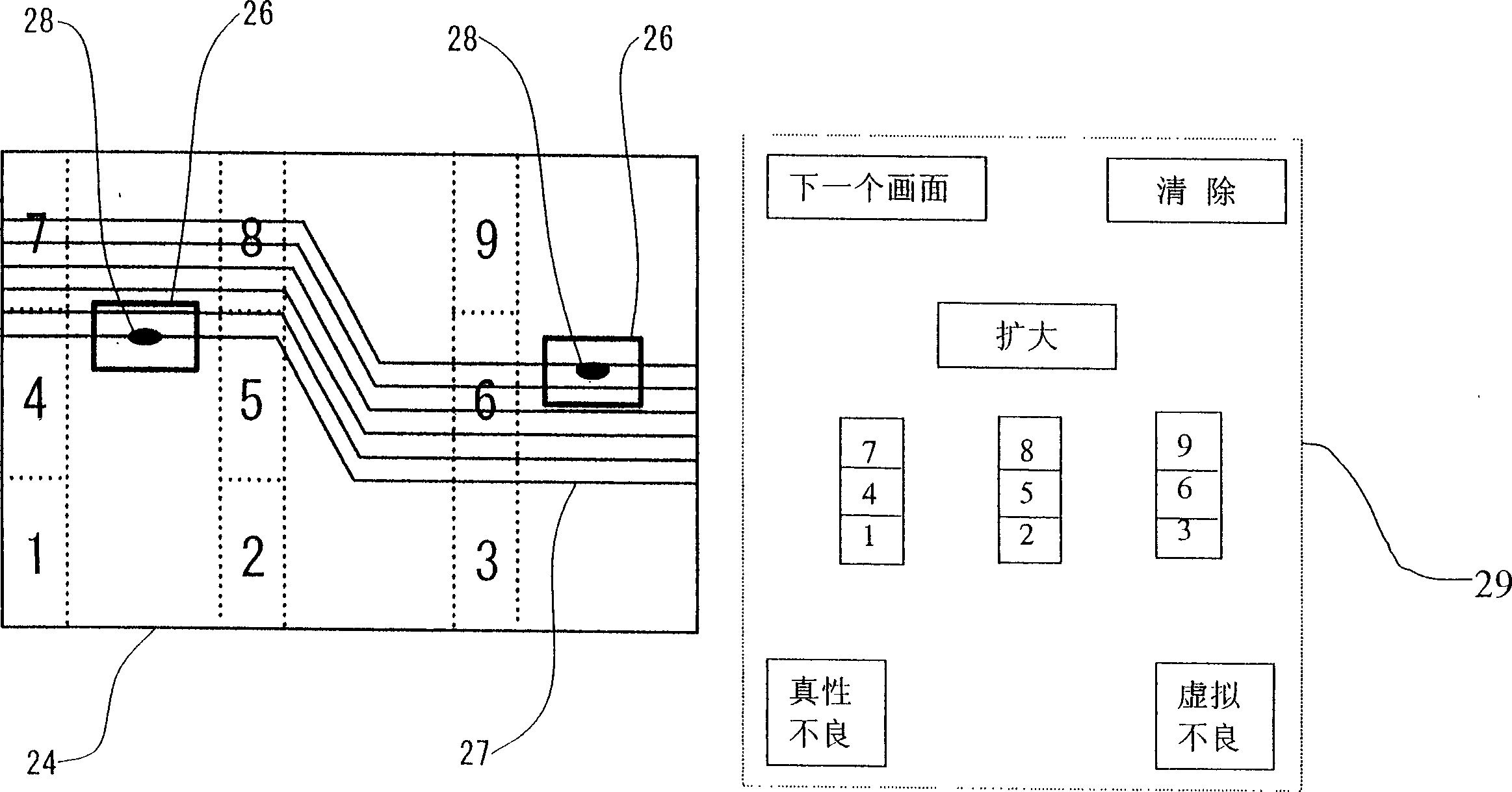
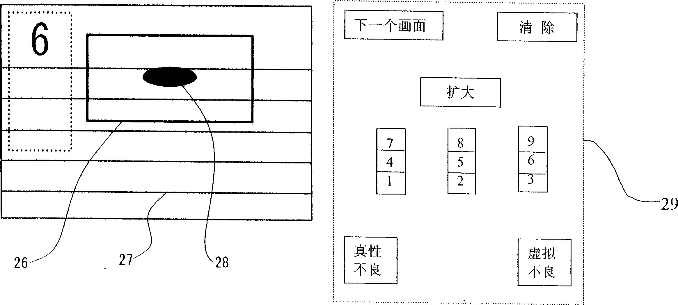
[0036] Hereinafter, embodiments of the present invention will be described with reference to the drawings. Image 6It is a schematic diagram of a schematic configuration of a printed circuit board inspection device for electronic component mounting (hereinafter, simply referred to as "inspection device") as one embodiment of the present invention. As shown in the figure, this detection device consists of an unwinding device for unwinding printed circuit boards for electronic component mounting (hereinafter, the detection of film carrier tapes for electronic component mounting such as TAB tapes (hereinafter referred to as film carrier tapes) will be described as an example) 11. It is used to detect defects in the circuit diagram of each component arranged in the longitudinal direction of the tape; and the image processing device 12, through image processing, determines that the circuit diagram of each component in the film carrier tape is defective, and calculates the defective ...


PUM


Abstract

Provided is a device for inspecting a film carrier tape for electronic component mounting which can efficiently discriminate true and pseudo failures, and also a method for confirming a pattern failure. This inspection device comprises a failure confirming unit. The confirming unit takes an image of one of image pickup zones etc. set as piece divisions in which a failure part of a wiring pattern detected by an image processor is positioned; displays the image pickup zone; and performs selective input operation to determine a visual discrimination result of whether at least one failure included in the displayed one image pickup zone is a true failure or all failure parts are pseudo failures. The images of the image pickup zones etc. including the failure parts are displayed in the decreasing order of sizes of the failure parts included in the image pickup zones.

Description

technical field [0001] The present invention relates to a detection device for printed circuit boards for electronic component mounting and a method for confirming pattern defects using the detection method, that is, for FPC and film carrier tape (TAB (Tape Automated Bonding) tapes, T-BGA (TapeBall Grid Array) tape, CSP (Chip Size Package) tape, ASIC (Application Specific Integrated Circuit) tape, COF (Chip On Film) tape, bimetallic (two-sided wiring) tape, multilayer wiring tape) Various parts of printed circuit boards for mounting electronic components, such as flexible printed circuit boards and hard printed circuit boards using materials such as glass fiber reinforced plastic substrates, have formed circuit diagrams. The image data obtained by photographing the parts is compared with the standard graphics. Thereby, defects in the circuit diagram are detected, and at the same time, detected defective parts are confirmed. It should be noted that the "printed circuit board f...

Claims


Application Information

Patent Timeline
IPC IPC(8): G01N21/956G01N21/84G01N21/95H01L21/60H05K13/08
CPCG01N21/95684H05K1/0269H05K13/081
Inventor 长谷川浩司埜藤幸雄关户启辅有马正浩
Owner MITSUI MINING & SMELTING CO LTD
Why Eureka
Try Eureka