

Electroluminescence device and its light-emitting layer and application
A technology for electroluminescent devices and light-emitting layers, which is applied in the fields of electro-solid devices, electrical components, semiconductor devices, etc., can solve problems such as the gap in luminous efficiency, and achieve the effect of improving luminous efficiency.
Active Publication Date: 2021-06-29
GUANGDONG JUHUA PRINTING DISPLAY TECH CO LTD
View PDF6 Cites 0 Cited by
- Summary
- Abstract
- Description
- Claims
- Application Information
AI Technical Summary
Problems solved by technology
[0006] Through the improvement of nanocrystalline semiconductor materials and the continuous optimization of QLED device structure, the performance of existing QLED devices has been greatly improved, but its luminous efficiency is still far from the requirements of industrial production.
Method used
View moreImage
Smart ImageViewing Examples

Examples
Embodiment 1
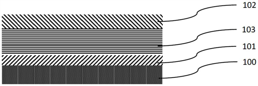
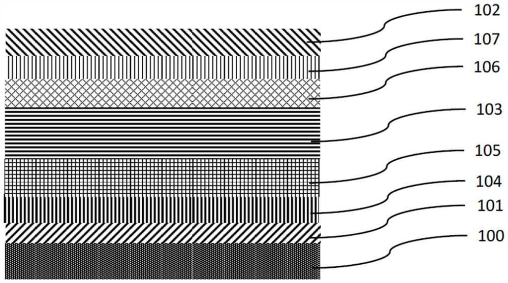
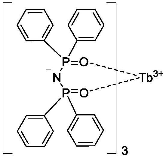
[0049] Embodiment 1: The device structure is: ITO / PEDOT:PSS / TFB / mCP:Tb(tpip) 3 :(CdSe / ZnS quantum dots) / PO-T2T / LiF / Al.
Embodiment 2
[0050] Embodiment 2: the device structure is: ITO / PEDOT:PSS / TFB / mCP:Tb(tpip) 3 :(CdSe / ZnS quantum rod) / PO-T2T / LiF / Al
Embodiment 3
[0051] Embodiment 3: the device structure is: ITO / PEDOT:PSS / TFB / mCP:Tb(tpip) 3 :(InP / ZnSeS quantum dots) / PO-T2T / LiF / Al
Login to View More PUM
| Property | Measurement | Unit |
|---|---|---|
| thickness | aaaaa | aaaaa |
| size | aaaaa | aaaaa |
| thickness | aaaaa | aaaaa |
Abstract
The present invention relates to a light-emitting layer of an electroluminescent device, comprising at least one nanocrystalline semiconductor material and at least one luminescent material of a lanthanide rare earth metal Tb complex; wherein, the luminescent material of the lanthanide rare earth metal Tb complex The emission peak wavelength is shorter than that of the nanocrystalline semiconductor material. The invention innovatively uses the luminescent material of the lanthanide rare earth metal Tb complex to cooperate with the nano-crystal semiconductor material, which facilitates the transfer of energy from the Tb complex luminescent material to the nano-crystal semiconductor material. At the same time, the rare earth element Tb in the luminescent material of the lanthanide rare earth metal Tb complex is a heavy metal, which has a strong spin-orbit coupling effect, and can efficiently utilize the singlet and triplet energy in the electroluminescent device at the same time, thereby Effectively improve the luminous efficiency of electroluminescent devices.
Description
technical field [0001] The invention relates to the technical field of light-emitting devices, in particular to an electroluminescence device, a light-emitting layer and applications thereof. Background technique [0002] Nanocrystalline semiconductor materials, also known as nanocrystals, are composed of a limited number of atoms, and at least two dimensions are on the order of nanometers. The two-dimensional space is restricted, and the quantum confinement effect is particularly significant. When excited by light or electricity, nanocrystalline semiconductor materials will emit a spectrum with a very narrow half-peak width (usually less than 40nm), and the luminous color is mainly determined by the particle size. Stability and other characteristics. [0003] Due to the advantages of high luminous efficiency, controllable luminous color, and high color purity, nanocrystalline semiconductor materials have great application potential in next-generation display technologies....
Claims
Login to View More Application Information
Patent Timeline
 Patent Type & AuthorityPatents(China)
IPC IPC(8): H01L51/50H01L51/54
CPCH10K85/351H10K50/115
Inventor李哲谢相伟宋晶尧付东
OwnerGUANGDONG JUHUA PRINTING DISPLAY TECH CO LTD