Memory devices having bit line precharge circuits and associated bit line precharge methods

A storage device, pre-charging technology, applied in static memory, digital memory information, information storage and other directions, can solve the problem of reducing the working speed of storage devices

Active Publication Date: 2005-02-02
SAMSUNG ELECTRONICS CO LTD
View PDF1 Cites 12 Cited by
  • Summary
  • Abstract
  • Description
  • Claims
  • Application Information

AI Technical Summary

Problems solved by technology

Therefore, the cut-off current may reduce the operating speed of the memory device

Method used

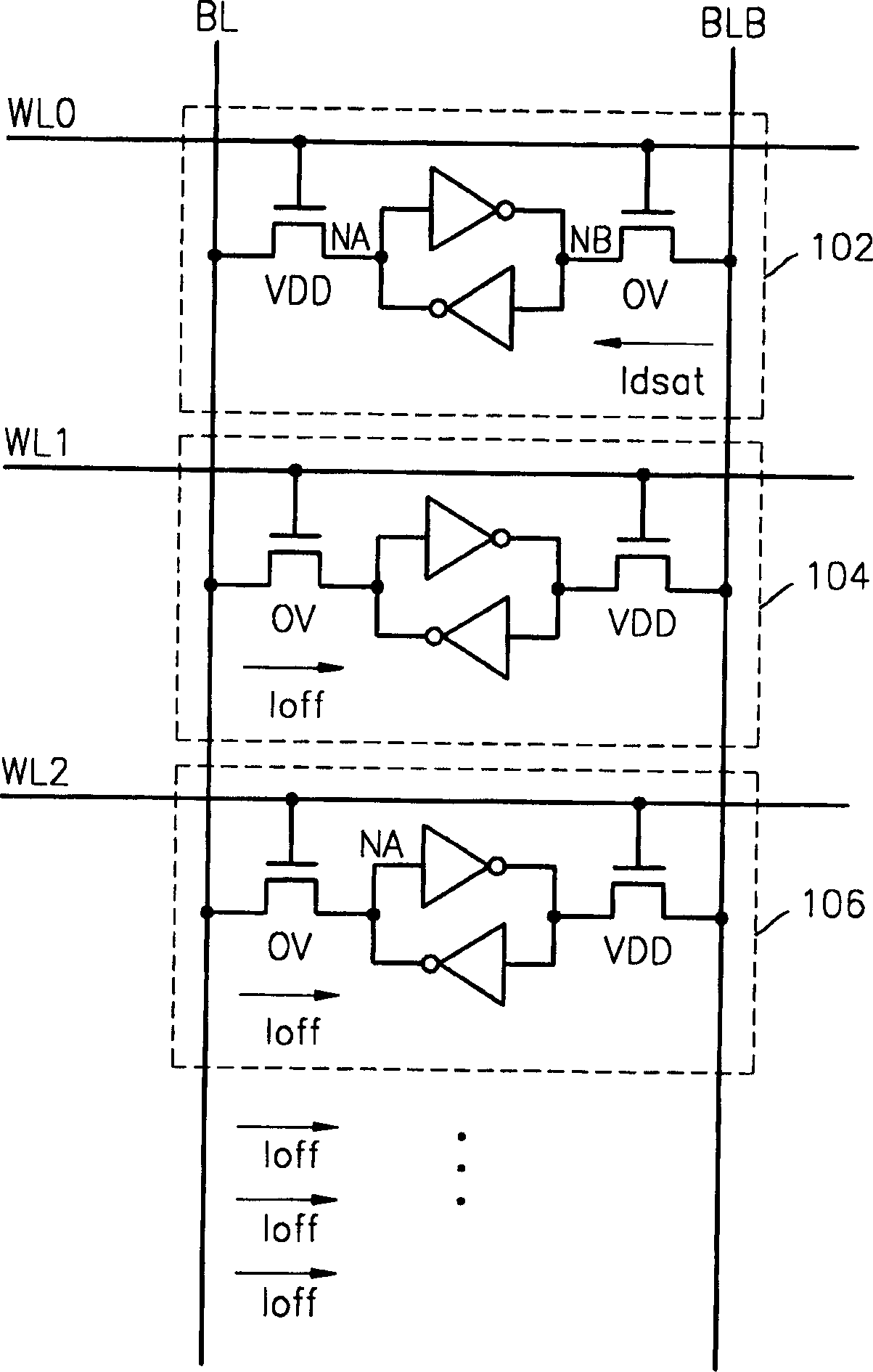
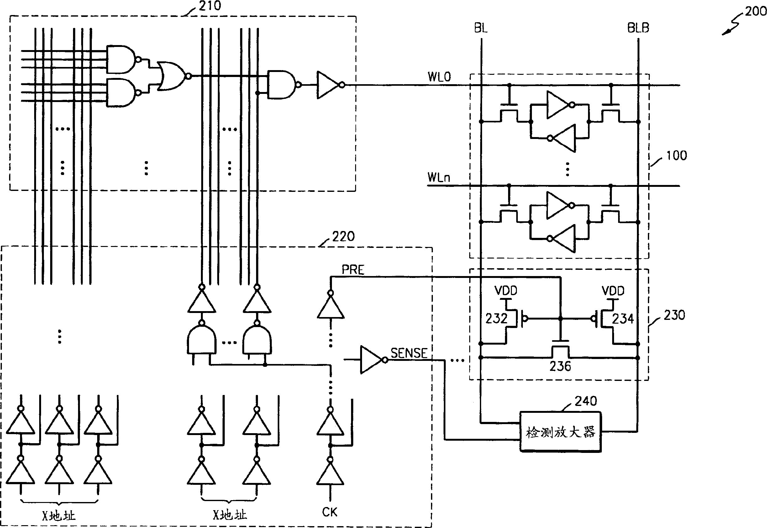
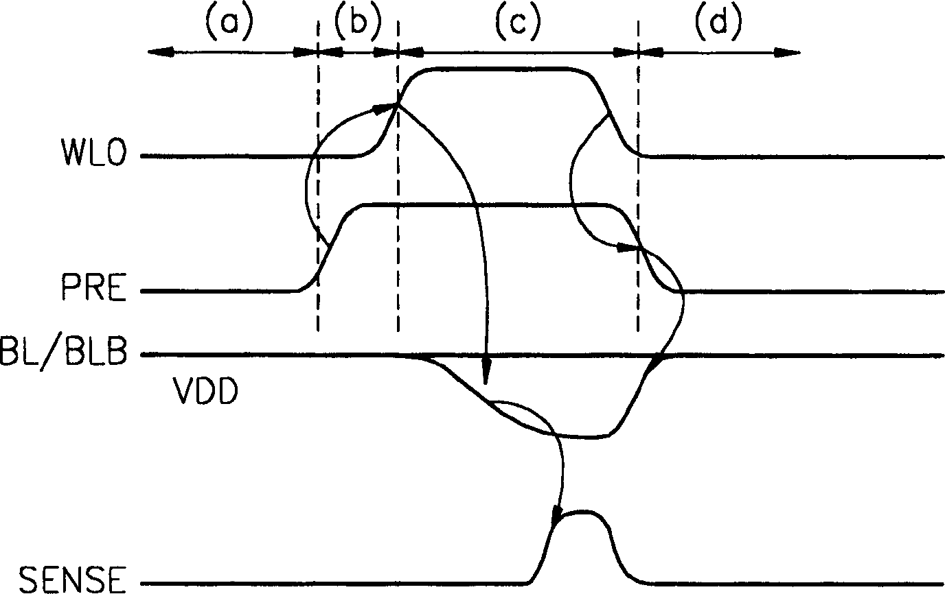

Image

  • Memory devices having bit line precharge circuits and associated bit line precharge methods
  • Memory devices having bit line precharge circuits and associated bit line precharge methods
  • Memory devices having bit line precharge circuits and associated bit line precharge methods

Examples


Embodiment Construction

[0027]The present invention will now be described more fully with reference to the accompanying drawings of exemplary embodiments of the invention. However, this invention may be embodied in many different forms and should not be construed as limited to the embodiments set forth herein. Moreover, these embodiments are provided so that this disclosure will be thorough and complete, and will fully convey the scope of the invention to those skilled in the art. Also, each embodiment described and illustrated herein includes its complementary conductivity type embodiment. Like reference numerals refer to like elements throughout.

[0028] Figure 4 Depicted are circuits and methods for generating a precharge signal (PRE). This precharge signal (PRE) is activated or disabled according to the precharge enable signal (PRE_EN). Such as Figure 4 As shown, the precharge enable signal (PRE_EN) is input into the delay circuit 410, which delays the precharge enable signal (PRE_EN) for...


PUM


Abstract

A memory device having an off-current (Ioff) robust precharge control circuit and a bit line precharge method are provided. The precharge control circuit may be embodied as a delay circuit unit which receives and delays a precharge enable signal for a predetermined delay time; a NAND gate which receives the precharge enable signal and the output of the delay circuit; and an inverter which inverts the output of the NAND gate. The precharge control circuit may enable the word lines before disabling the precharge signal.

Description

[0001] Related literature [0002] This application claims priority under 35 U.S.C § 119 to Korean Patent Application No. 2003-36748 filed on June 9, 2003, the entire disclosure of which is incorporated herein by reference. field of invention [0003] The present invention relates to a semiconductor storage device, in particular to a semiconductor storage device with a bit line precharging circuit and a related bit line precharging method. Background of the invention [0004] With the advancement of semiconductor storage process technology, smaller and smaller semiconductor storage devices appear. Deep submicron processes are now being developed to facilitate the production of small, highly integrated memory devices. In order to improve the performance of developed transistors using deep sub-micron technology, this reduces the threshold voltage (Vth) of the transistor. However, when the threshold voltage is lowered, it increases the saturation current of the transistor in ...

Claims


Application Information

Patent Timeline
Patent Type & Authority Applications(China)
IPC IPC(8): G11C7/06G11C7/12
CPCG11C7/06G11C7/12
Inventor 宋泰中
Owner SAMSUNG ELECTRONICS CO LTD
Why Eureka
Try Eureka