Semiconductor device

A technology for semiconductors and devices, applied in the field of semiconductor devices, can solve problems such as no disclosure, and achieve the effects of suppressing the decline of bonding and reducing damage

Inactive Publication Date: 2005-02-02
RENESAS TECH CORP
View PDF2 Cites 8 Cited by
  • Summary
  • Abstract
  • Description
  • Claims
  • Application Information

AI Technical Summary

Problems solved by technology

Therefore, it is necessary to implement narrow-pitch wire bonding to the hard bonding pads conventionally formed on a very soft substrate insulating material, and no countermeasures are disclosed in the above-mentioned known examples.

Method used


Image

  • Semiconductor device
  • Semiconductor device
  • Semiconductor device

Examples


Embodiment Construction

[0039] Embodiments of the present invention will be described below. In addition, this invention is not limited to the form described in this specification, It does not prevent correction|amendment based on the conventional well-known technique or the technique which becomes a well-known technique.

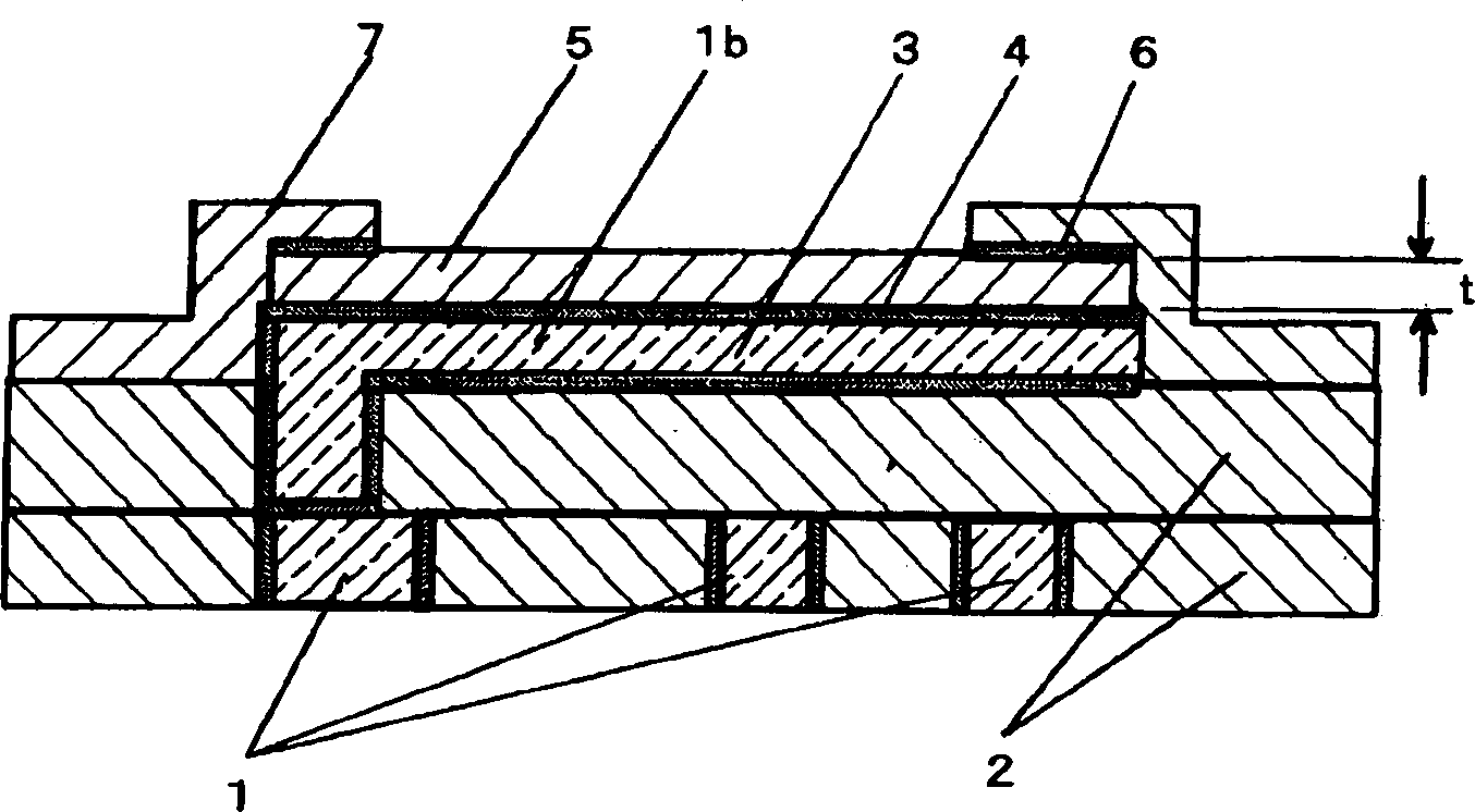
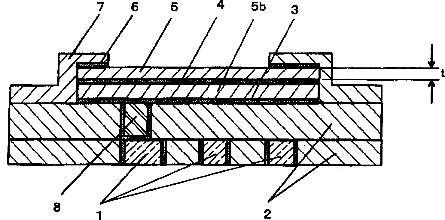
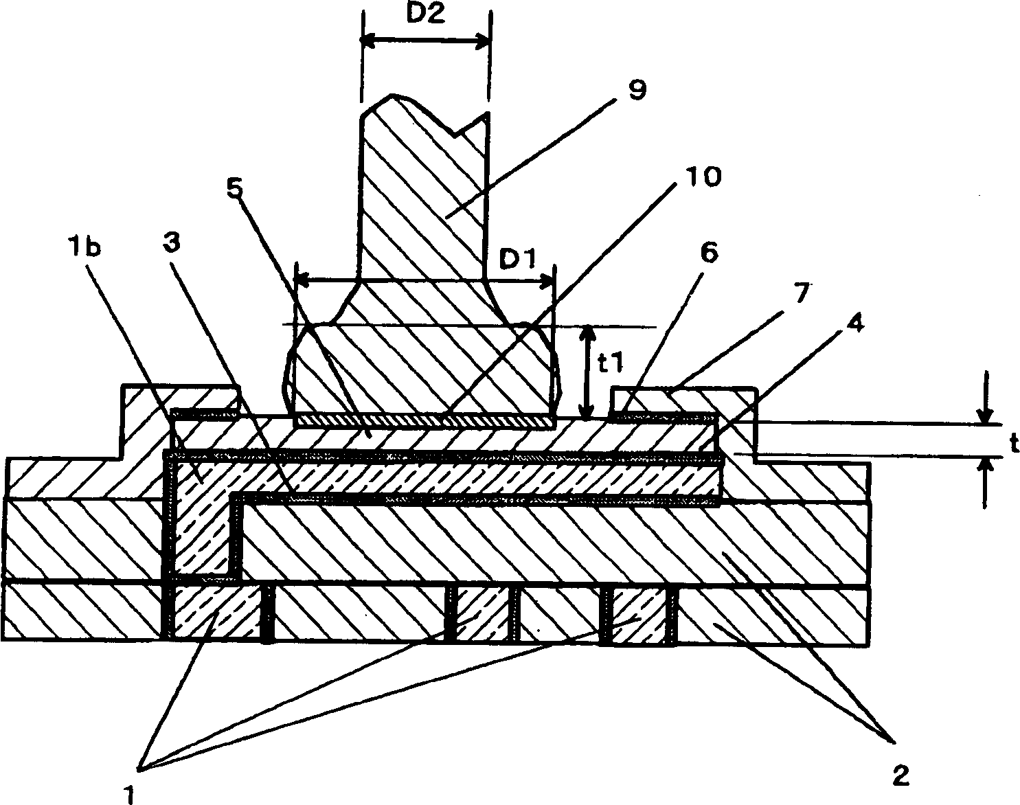
[0040] figure 1 is a cross-sectional view showing the bonding pad structure on the surface of the LSI according to the first embodiment of the present invention. In this embodiment, an example of a method of connecting a semiconductor device and an external device by a bonding wire is shown.

[0041]Compared with SiO, an interlayer insulating film formed of a low-dielectric insulating material (here, SiOC as an example) is formed on a semiconductor substrate (here, as an example, Si is used). A plurality of Cu wirings 1 are included thereon. An interlayer insulating film 2 covering the Cu wiring 1 on the Cu wiring 1 is formed thereon, and a Cu bonding wiring layer 1 b serving a...


PUM


Abstract

An object of the present invention is to establish, for an LSI having a stacked interconnection structure of Cu interconnect / Low-k material, a narrow pitch wire bonding technique enabling a reduction in damage to a bonding pad and application similar to the conventional LSI of an aluminum interconnection. In a semiconductor device having a multilayer interconnection made of a Cu interconnect / Low-k dielectric material, the above-described object can be attained by a bonding pad structure in which all the wiring layers up to the uppermost cap interconnect are formed of a Cu wiring layer and a bonding pad portion formed of a Cu layer is equipped with a refractory intermediate metal layer such as Ti (titanium) filmor (tungsten) film on the Cu layer and an aluminum alloy layer on the intermediate metal layer.

Description

technical field [0001] The present invention relates to semiconductor devices. Background technique [0002] Hitherto, aluminum alloy wiring has been used for wiring between semiconductor elements in a semiconductor device, and connection members such as bonding wires have been used for electrical connection to the outside. In order to suppress the deterioration of the soundness of the connection of these connection members, for example, in the invention disclosed in (Japanese) Unexamined Patent Publication No. 5-6915 (Patent Document 1), a bonding wire connection on a semiconductor substrate covered with an insulating film is In the structure of the electrode pad part, the following structure is proposed: the insulating film is composed of SiO film or phosphate silicon glass (PSG), and the electrode pad is composed of three layers: the lower layer is an Al film, the middle layer is a Ti compound film, and the upper layer is an Al film. The structural composition prevents d...

Claims


Application Information

Patent Timeline
Patent Type & Authority Applications(China)
IPC IPC(8): H01L23/52H01L21/3205H01L21/44H01L21/56H01L21/60H01L21/768H01L23/31H01L23/48H01L23/485H01L23/532H01L25/065
CPCH01L2924/20303H01L2924/0105H01L2224/05624H01L24/78H01L2224/4851H01L2924/20107H01L2225/06558H01L2924/15311H01L23/3128H01L2224/85045H01L2924/01022H01L2224/02166H01L2224/48091H01L2924/01013H01L2224/32225H01L2224/45015H01L2924/20751H01L24/48H01L24/45H01L2924/19043H01L2224/1134H01L2225/06568H01L2224/4807H01L2224/73204H01L2224/48247H01L24/85H01L2924/01033H01L2224/32145H01L2924/20305H01L2924/01074H01L2924/01078H01L25/0657H01L2224/16225H01L2924/20106H01L23/53238H01L2924/01015H01L2224/85205H01L2224/48624H01L2924/01082H01L2924/01004H01L21/563H01L2224/32245H01L2924/01019H01L2224/13144H01L2924/01029H01L2924/00013H01L2224/48453H01L2924/01105H01L2924/014H01L24/03H01L2224/78301H01L2924/05042H01L2924/04941H01L2924/01079H01L2224/48465H01L24/05H01L24/13H01L24/16H01L2224/48227H01L2224/04042H01L2924/14H01L2924/01006H01L2924/20304H01L2924/0102H01L2924/01014H01L2924/20105H01L2224/45144H01L2224/73265H01L24/73H01L2224/023H01L2224/0401H01L2224/73253H01L2924/181H01L2924/00014H01L2224/13099H01L2924/00H01L2924/00012H01L2924/00011H01L2924/00015H01L2924/0001H01L21/60
Inventor 田中直敬岩崎富生三浦英生中岛靖之松泽朝夫
Owner RENESAS TECH CORP
Why Eureka
Try Eureka