Method for preparing polycrystalline silicon layer and light shield

A technology of polysilicon layer and amorphous silicon layer is applied in the field of photomask, which can solve the problems of increasing process steps and process cost, low utilization rate of laser light 16, etc.

Active Publication Date: 2005-05-11
AU OPTRONICS CORP
View PDF0 Cites 2 Cited by
  • Summary
  • Abstract
  • Description
  • Claims
  • Application Information

AI Technical Summary

Problems solved by technology

In addition, the polysilicon layer 13 crystallized by the laser tempering method has many defects 13a on the crystal lattice or grain boundary 13b.
Although the second laser light 16 irradiation or high temperature treatment can be used to repair the defect 13a, this will increase the process steps and process cost
In addition, since only part of the laser light 16 penetrates the light-transmitting region 15c to melt the amorphous silicon layer 12, another part of the laser light 16 will be partially reflected and partially absorbed by the light-impermeable region 15a and converted into heat. , leading to low utilization rate of laser light 16

Method used


Image

  • Method for preparing polycrystalline silicon layer and light shield
  • Method for preparing polycrystalline silicon layer and light shield
  • Method for preparing polycrystalline silicon layer and light shield

Examples


Embodiment 1

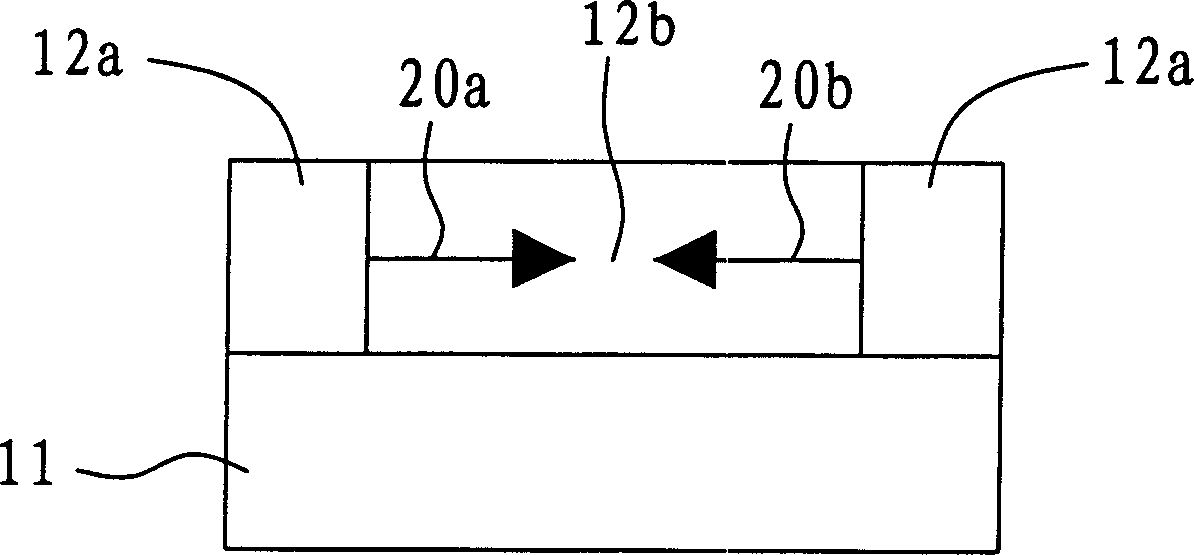
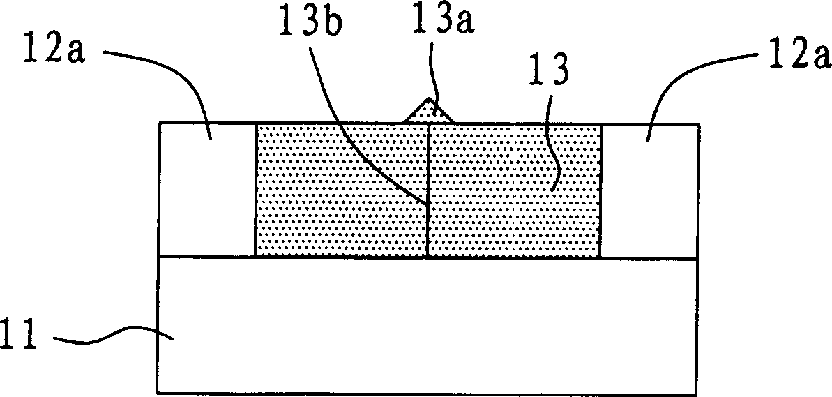
[0015] Please refer to figure 2 and Figure 3A-3E , figure 2 is a flowchart of a method for manufacturing a polysilicon layer according to Embodiment 1 of the present invention, Figures 3A to 3E is a cross-sectional flow diagram of a method for manufacturing a polysilicon layer according to Embodiment 1 of the present invention. First, in step 21, a substrate 21 is provided, such as Figure 3A shown. Next, enter figure 2 In step 22, an amorphous silicon layer 32 is formed on the substrate 31, the amorphous silicon layer 32 has at least a first amorphous silicon region 32a and a second amorphous silicon region 32b, such as Figure 3B shown. Then, enter step 23, fully melt the first amorphous silicon region 32a and preheat the second amorphous silicon region 32b, as Figure 3C Shown; The first amorphous silicon region 32a that is fully melted is crystallized into a first polysilicon layer 33a, as Figure 3D shown.

[0016] In order to achieve the purpose of fully me...

Embodiment 2

[0023] Please refer to Figure 5 , which is a top view of a photomask used for laser light preheating and melting of an amorphous silicon layer according to Embodiment 2 of the present invention. exist Figure 5 Among them, the photomask 55 is used for preheating and melting an amorphous silicon layer on a substrate for a laser light, the amorphous silicon layer has a first amorphous silicon region and a second amorphous silicon region, and the photomask 55 is Move relative to the substrate. The techniques of forming the amorphous silicon layer on the substrate and moving the photomask relative to the substrate in this embodiment have been disclosed in Embodiment 1, and will not be repeated here. The photomask 55 includes a photomask body 55b, an opaque area 55a, a first photomask pattern 56, a second photomask pattern 57 and a second part of the translucent area 55d, the opaque area 55a is formed on on the mask body 55b. The first mask pattern 56, the second mask pattern ...


PUM


Abstract

The method includes following steps: firstly in base board, amorphous silicon has first amorphous silicon area and second amorphous silicon area; next a photomask is provided, the photomask consists of partly photo zone and photo zone; the partly photo zone and photo zone each relates to second amorphous silicon area and first amorphous silicon area. Laser is used to illuminate the photomask so that the first amorphous silicon area is entirely melted and the second amorphous is preheated; the melted first amorphous silicon area and the second preheated amorphous silicon are crystallized to form first polycrystalline silicon layer; the photomask and base board are moved to make the photo zone to correspond to the preheated second amorphous silicon area; laser is used to illuminate the photomask for making the preheated second amorphous silicon area to entirely melt so that the melted second amorphous silicon area will crystallize second polycrystalline silicon layer.

Description

technical field [0001] The present invention relates to a method for manufacturing a polysilicon layer, and in particular to a method for manufacturing a polysilicon layer that uses a photomask to allow laser light to preheat an amorphous silicon layer and completely melts the preheated amorphous silicon layer, and in the method The reticle used in the method. Background technique [0002] In today's era of rapid technological development, display panels have been widely used in portable electronic devices such as notebook computers, personal digital assistants, and mobile phones. Among them, the display panel can be divided into a non-polysilicon (a-Si) thin film transistor (thin film transistor, TFT) display panel and a low temperature polysilicon (LTPS) TFT display panel. The biggest difference between the LTPSTFT display panel and the a-Si TFT display panel is that the LTPS TFT display panel converts the a-Si layer into a polysilicon layer by laser annealing (Laser Anne...

Claims


Application Information

Patent Timeline
IPC IPC(8): C30B13/00G03F1/38H01L21/00H01L21/20
Inventor 孙铭伟
Owner AU OPTRONICS CORP
Why Eureka
Try Eureka