Method for producing ternary signal and circuit device

A circuit configuration, signal level technology, applied in the direction of logic circuit connection/interface layout, logic circuit, transmission line coupling device, etc., to achieve the effect of reducing effort and expenditure, small surface area, and avoiding overvoltage protection problems

Inactive Publication Date: 2005-05-18
INFINEON TECH AG
View PDF0 Cites 1 Cited by
  • Summary
  • Abstract
  • Description
  • Claims
  • Application Information

AI Technical Summary

Problems solved by technology

[0005] As another option, instead of generating a lower voltage internally, a lower, or higher, voltage can be introduced externally, for example, with a semiconductor module having an internal operating voltage of 1.5V, which is possible Introduce a voltage of 3.3V from the outside, and in many circuit environments, in addition to the lower internal operating voltage of the semiconductor modules, a higher external operating voltage is also available, however, in order to use the external If the operating voltage is conducted into the semiconductor module, an additional connection pin is required, which, moreover, in this case raises a problem with regard to the overvoltage protection of the internal structure of the semiconductor module

Method used


Image

  • Method for producing ternary signal and circuit device
  • Method for producing ternary signal and circuit device
  • Method for producing ternary signal and circuit device

Examples


Embodiment Construction

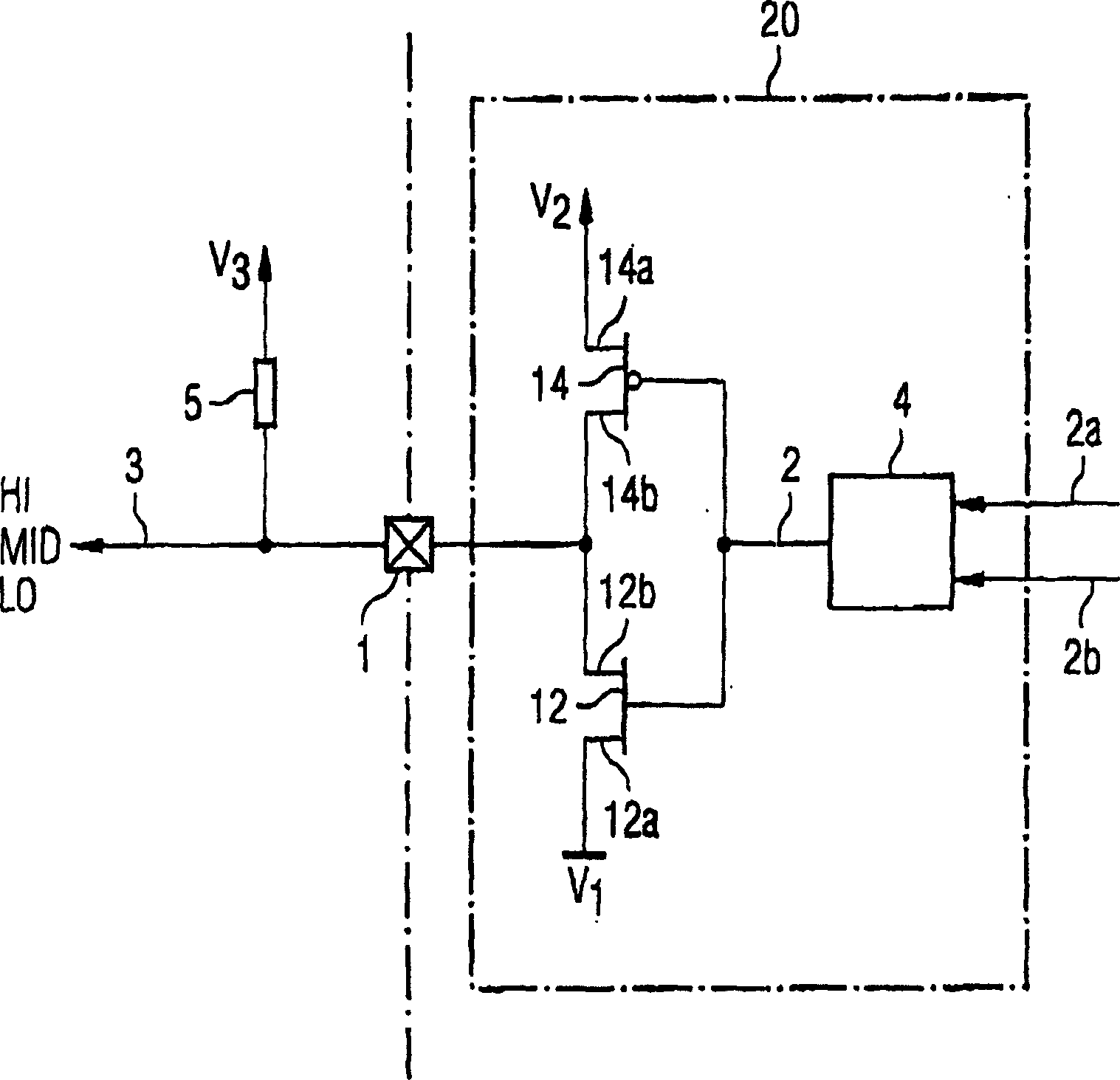
[0019] For this purpose, the output structure 20 comprises switching means and is in the form of a first transistor 12 and a second transistor 14 . In this embodiment, the transistors 12, 14 are field effect transistors connected in series, and the charge carriers of the transistors 12, 14 are formed in such a way that the transistors 12, 14 would form an inverter structure selection, therefore, in order to achieve this idea, the control voltage connections of the transistors 12, 14 are connected to each other, the first transistor 12 is connected to a voltage with a first potential V 1 A connection 12a, and wherein, the potential V 1 is a ground potential, and a further connection 12b of the first transistor 12 is then connected to a signal output terminal 1 of the semiconductor module and to a connection 14b of the second transistor 14, and then, the A further connection 14b of the second transistor 14 will be connected to a second potential V 2 , and where the second pote...


PUM


Abstract

According to a method for generating a ternary signal, a first signal level (LO) is generated by the signal output (1), wherein the signal output (1) is connected to a first potential (V1). A second signal level (MID) is generated, and wherein the signal output is connected to a second potential (V2). And in order to generate a third signal level (HI), the signal output terminal (1) is connected to a third potential (V3) through a resistance device, so when the signal output terminal (1) is connected from the first When a potential (V1) and the second potential (V2) are decoupled, the electrical three signal level (HI) will be generated, wherein the first potential (V1) can be a ground potential, and the second potential ( V2 ) can be an operating voltage of a semiconductor module, and the third potential ( V3 ) can be an external operating voltage.

Description

technical field [0001] The invention relates to a method and a circuit arrangement for generating a ternary signal, in particular at the output structure of a semiconductor module. Background technique [0002] Ternary interfaces, that is, signal outputs with three active states, are used especially with semiconductor modules having a small number of connections, and with special similar semiconductor modules, for example, line drivers, whereby the ternary signal With the use of the outputs, in particular the number of connections, for example in the form of connection pins, the semiconductor module can be reduced and thus cost savings can also be achieved. [0003] The three active states in the form of three different signal levels are schematically represented in FIG. 2 . The different signal levels, HI, MID, LO, can be, for example, voltages derived from one operating voltage of a circuit, while increasingly smaller operating voltages are used with semiconductor modules...

Claims


Application Information

Patent Timeline
Patent Type & Authority Applications(China)
IPC IPC(8): H03K17/687H03K19/00H03K19/0185H03M5/16H04L25/02
CPCH04L25/028
Inventor J·霍赫尔P·佩斯
Owner INFINEON TECH AG
Why Eureka
Try Eureka