Semiconductor device with a pair of radiating fan
A semiconductor and heat sink technology, applied in semiconductor devices, semiconductor/solid-state device components, electrical solid-state devices, etc., can solve the problems of uneven heat dissipation path of semiconductor components, insufficient heat dissipation performance, etc., to avoid poor work, prevent Contact, the effect of preventing the decrease in durability
- Summary
- Abstract
- Description
- Claims
- Application Information
AI Technical Summary
Problems solved by technology
Method used
Image
Examples
no. 1 example
[0030] The inventors have previously studied semiconductor devices having upper and lower surface cooling structures. Figure 9 An example of a semiconductor element (power element) used in a semiconductor device is shown in . As we all know, the Figure 9 The semiconductor element 1 shown in the prior art is used as a general-purpose power element (for example, an IGBT) for cooling on one side. A collector electrode is formed on the entire lower surface of the semiconductor element 1, and the collector electrode is soldered to a lower heat sink.
[0031] On the other hand, if Figure 9 As shown, a plurality of rectangular emitter electrodes 2 are formed on the upper surface of the above-mentioned semiconductor element 1 , and heat radiation blocks 3 are soldered to these emitter electrodes 2 . Here, the size of the range of the emitter electrode 2 (that is, the protective film opening) is smaller than the size of the main cell (emitter main cell portion) 4 which is the ran...
no. 2 example
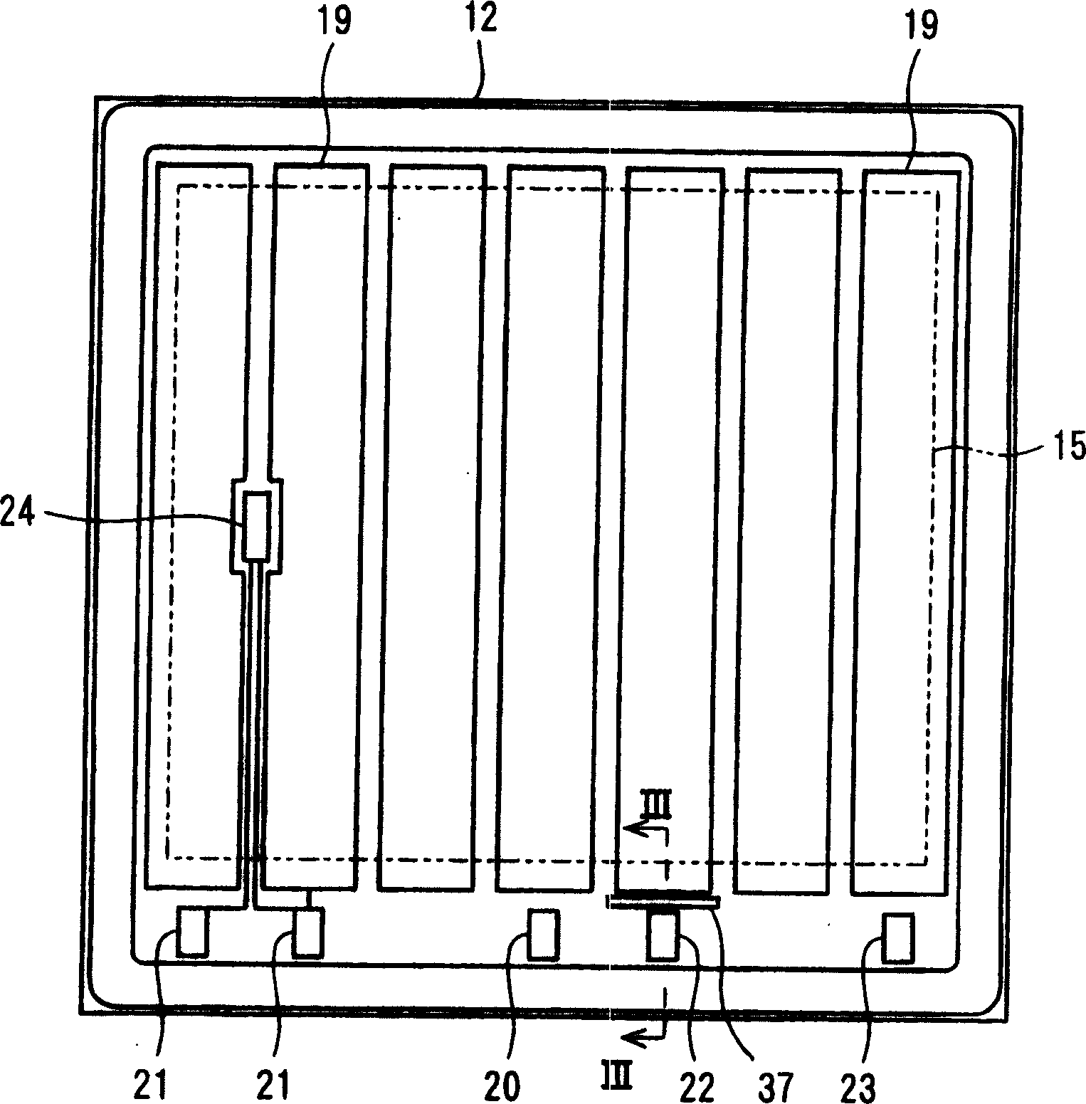
[0062] Image 6 is a diagram showing a part of a semiconductor device according to a second embodiment of the present invention. In this semiconductor device, while disposing the main unit region 19 on the lower surface of the heat sink block 15, it is formed at a position within a range of approximately 1.0 mm from the end of the solder layer 16 to be bonded to the heat sink block 15. . Specifically, Image 6 The dimension d1 (the distance between the end of the solder layer 16 and the end of the main cell region 19 ) shown in , is 1.0 mm or less. again, in Image 6 In , the layer indicated by reference numeral 39 is, for example, an electrode for a surface solder layer made of TiNiAu.
[0063] With such a configuration, it is possible to arrange the main cell region 19 on the upper surface of the semiconductor chip 12, that is, the channel formation region of the main cell or the region where the channel current flows in the main cell, under the heat sink block 15. At t...
no. 3 example
[0068] Figure 7 is a diagram showing a semiconductor element in a semiconductor device according to a third embodiment of the present invention. In this semiconductor element, the signal line connection plate and the current mirror portion are collectively arranged at one place on the upper surface of the semiconductor chip 12 .
[0069] Specifically, the signal electrodes 20 , 21 , 22 , 23 (signal line connection plates) and the current detection region 37 (current mirror portion) are collectively arranged on the left half of the lower side of the upper surface of the semiconductor chip 12 .
[0070] In this way, the heat dissipation path of the heat generated in the main cell region 19 becomes the vertical direction of the semiconductor chip 12, and sufficient heat dissipation performance can be obtained, thereby effectively preventing an increase in element temperature.
[0071] In addition, since the signal line connection plate and the current mirror are collectively arra...
PUM
 Abstract
Description
Claims
Application Information


