Thermal interfacial material and method of manufacture

A technology of thermal interface material and manufacturing method, applied in electrical components, electrical solid devices, circuits, etc., can solve the problems of uniformity of thermal conduction, increase in volume, lack of flexibility of thermal interface materials, etc., to improve efficiency and stability. Effect

Inactive Publication Date: 2005-09-14
HONG FU JIN PRECISION IND (SHENZHEN) CO LTD +1
View PDF1 Cites 10 Cited by
  • Summary
  • Abstract
  • Description
  • Claims
  • Application Information

AI Technical Summary

Problems solved by technology

However, the thermal interface material produced by this method has disadvantages. First, the thickness of the thermal interface material produced by injection molding is relatively large. Although the thermal conductivity of the thermal interface material is high, the volume of the thermal interface material increases. It is not compatible with the trend of device miniaturization, and the thermal interface material lacks

Method used


Image

  • Thermal interfacial material and method of manufacture
  • Thermal interfacial material and method of manufacture
  • Thermal interfacial material and method of manufacture

Examples


Embodiment Construction

[0021] The present invention will be described in detail below in conjunction with the accompanying drawings and specific embodiments.

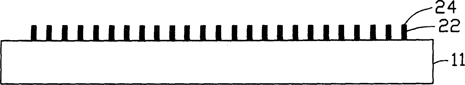
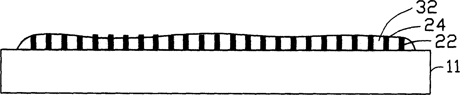
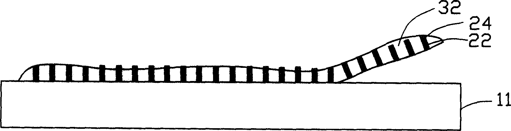
[0022] see figure 1 , is an aligned carbon nanotube array 22 filled with nano-silver material 24 provided by the present invention, wherein the carbon nanotube array 22 is formed on a substrate 11, a plurality of carbon nanotubes are substantially parallel to each other, and are substantially parallel to the substrate 11 vertical.

[0023] The preparation method of the carbon nanotube array 22 filled with nano-silver material 24 of the present invention is as follows: firstly, a catalyst layer is evenly deposited on the surface of the substrate 11, and the method can be completed by thermal deposition, electron beam deposition or sputtering. The material of the substrate 11 can be glass, quartz, silicon or alumina. In this embodiment, porous silicon is used, the surface of which is a porous layer, and the diameter of the pores is extremely ...


PUM

PropertyMeasurementUnit
Particle sizeaaaaaaaaaa
Thicknessaaaaaaaaaa
Viscosityaaaaaaaaaa

Abstract

A heat interface material based on carbon nm tube heat conduction includes an Ag glue matrix constituting a first surface, a second surface corresponding to the first and multiple parallel carbon nm tubes extending from the first surface to the second which are filled with nm Ag material composed of pure Ag particles, borazon particles and artificial oil and formed in a post due to the limit by the shape of the tube. A manufacturing method is provided including the following steps: providing a carbon nm tube array filled with nm Ag material, coating and infiltrating the array with the Ag glue, solidifying the Ag glue to form a heat interface material.

Description

【Technical field】 [0001] The invention relates to a thermal interface material and a manufacturing method thereof, in particular to a thermal interface material using carbon nanotubes for heat conduction and a manufacturing method thereof. 【Background technique】 [0002] In recent years, with the rapid development of semiconductor device integration technology, the integration degree of semiconductor devices is getting higher and higher. However, as devices become smaller and smaller, their heat dissipation requirements become higher and higher, becoming an increasingly important issue. In order to meet this need, various heat dissipation methods such as fan heat dissipation, water-cooled auxiliary heat dissipation, and heat pipe heat dissipation are widely used, and a certain heat dissipation effect has been achieved. However, due to the uneven contact interface between the heat sink and the semiconductor integrated device, the general mutual contact area is less than 2 %,...

Claims


Application Information

Patent Timeline
IPC IPC(8): H01L23/373
Inventor 吕昌岳余泰成陈杰良
Owner HONG FU JIN PRECISION IND (SHENZHEN) CO LTD
Why Eureka
Try Eureka