Bulk silicon mirrors with hinges underneath
A hinge, single crystal silicon technology, applied in the photoengraving process of the pattern surface, the microstructure device composed of deformable elements, the instrument, etc., can solve the problems of lack of overall structure and difficult alignment, and achieve high performance Powerful, wide-ranging effects
- Summary
- Abstract
- Description
- Claims
- Application Information
AI Technical Summary
Problems solved by technology
Method used
Image

Examples
Embodiment Construction
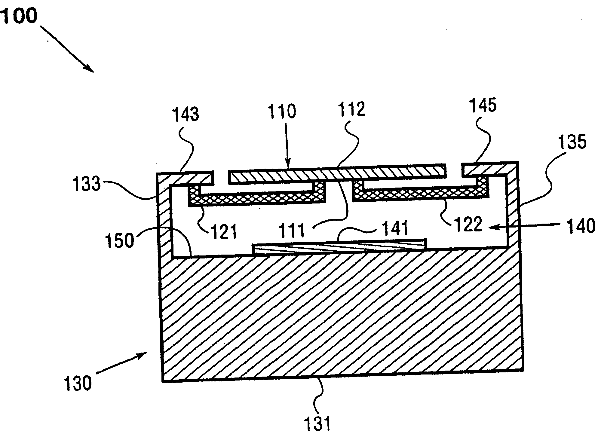
[0022] Figures 1A-1B A first embodiment of a MEMS device according to the invention is shown. Figure 1A A schematic side sectional view of MEMS device 100 is shown, which includes body element 110 ; first and second hinge elements 121 , 122 ; and support 130 . Bulk element 110 may have a "device" (or "top") surface 112 , and a "bottom" surface 111 positioned below and opposite device surface 112 . Each of the first and second hinge elements 121 , 122 is disposed below the device surface 112 . as Figure 1A In the implementation of the embodiment, the hinge elements 121 , 122 are each connected at one end to the bottom surface 111 of the body element 110 and at the other end to the support 130 . In this way, the body element 110 is suspended by the hinge elements 121 , 122 arranged entirely below the component surface 112 .
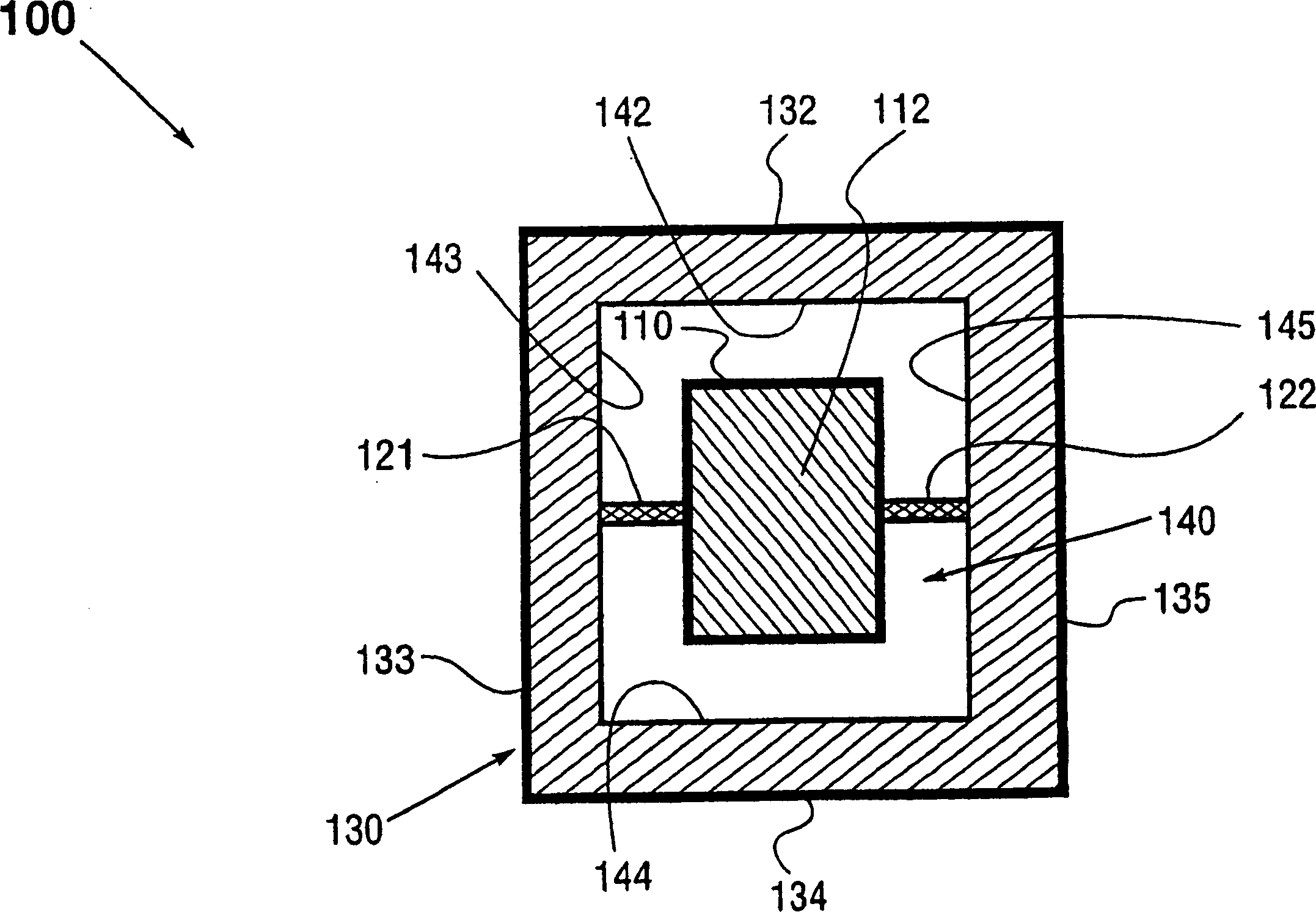
[0023] Figure 1B A schematic top view of the MEMS device 100 is shown. By way of example, it is shown that the device surface 112 of the bulk eleme...
PUM
 Abstract
Description
Claims
Application Information