Ridged wave-guiding high-power semiconductor laser structure with conical gain zone

A technology of tapered gain region and ridge waveguide, which is applied in the field of ridge waveguide high-power semiconductor laser structure, can solve the problems of semiconductor laser maximum output power and beam quality limitation, multiple side modes, etc.

Inactive Publication Date: 2005-10-12
INST OF SEMICONDUCTORS - CHINESE ACAD OF SCI
View PDF0 Cites 9 Cited by
  • Summary
  • Abstract
  • Description
  • Claims
  • Application Information

AI Technical Summary

Problems solved by technology

Simply increasing the stripe width can reduce the beam width and increase the optical power, but it is easy to generate multiple side modes, which greatly limits the maximum output power and beam quality of semiconductor lasers

Method used


Image

  • Ridged wave-guiding high-power semiconductor laser structure with conical gain zone
  • Ridged wave-guiding high-power semiconductor laser structure with conical gain zone
  • Ridged wave-guiding high-power semiconductor laser structure with conical gain zone

Examples


Embodiment Construction

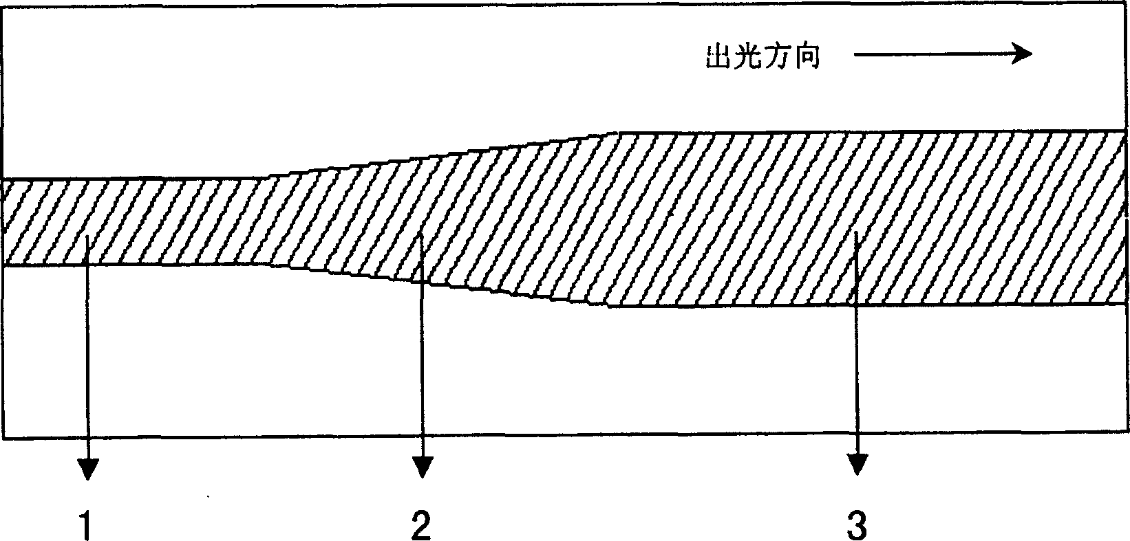
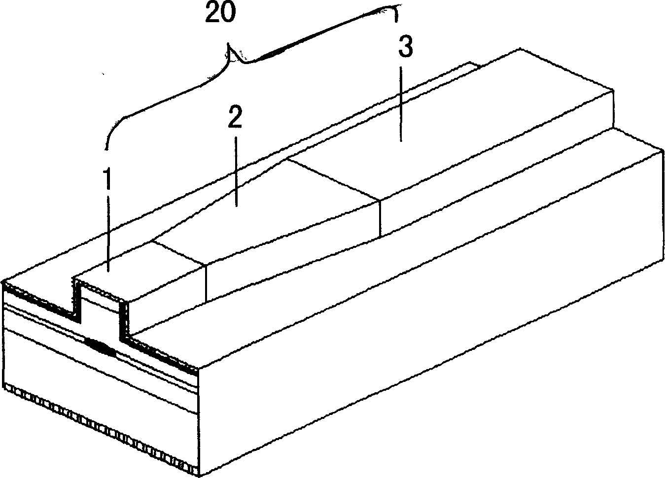
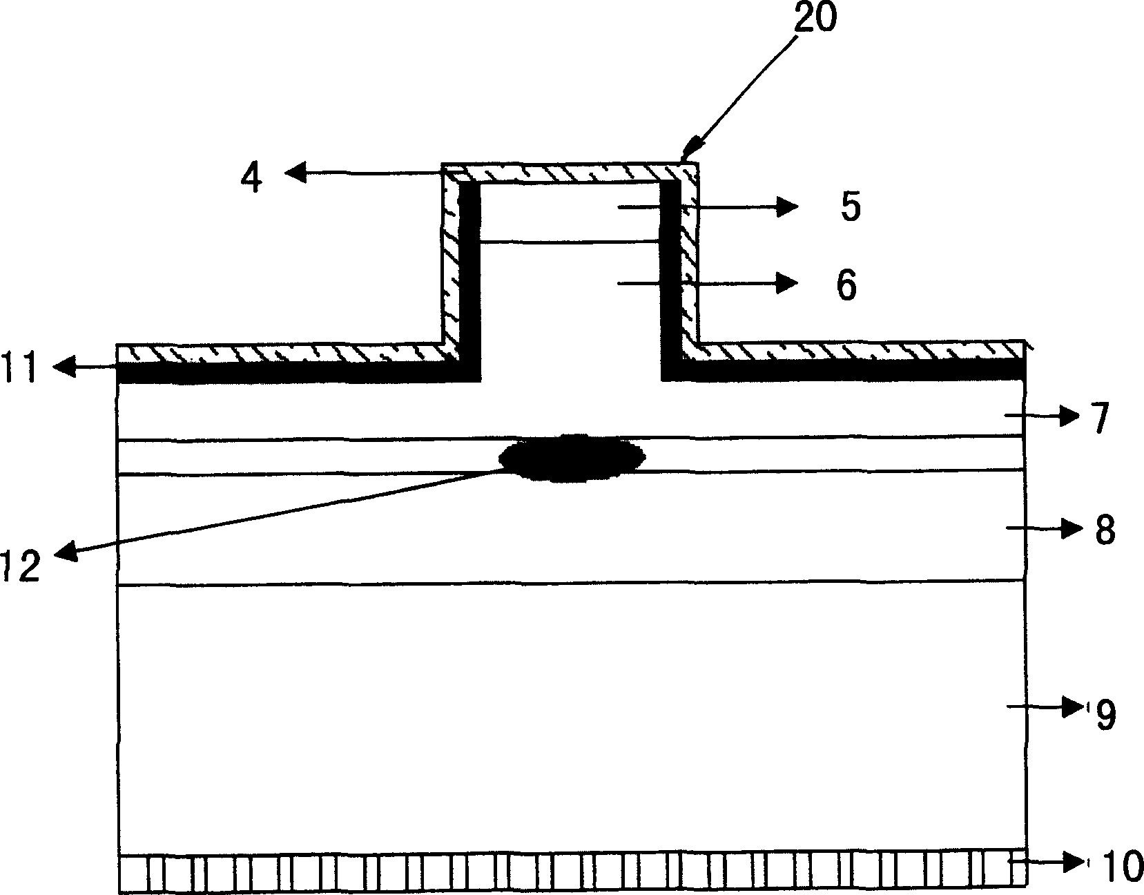
[0030] see figure 1 , figure 2 and image 3 As shown, the present invention has a ridge waveguide high-power semiconductor laser structure with a tapered gain region, which is characterized in that it includes:

[0031] a substrate 9, the substrate 9 is an indium phosphorus material;

[0032] An AlGaAs layer 8, the AlGaAs layer 8 is fabricated on the substrate 9, and the AlGaAs layer 8 is N-type doped;

[0033] An AlGaInAs active layer 12, the AlGaInAs AlGaInAs active layer 12 is fabricated on the AlGaAs 8, the AlGaInAs active layer 12 is a respectively constrained strained quantum well structure, lasing The wavelength is 14xxnm;

[0034] An AlInAs layer 7, the AlInAsAlInAs layer 7 is fabricated on the AlGaInAs active layer 12, and the AlInAs layer 7 is P-type doped;

[0035] An indium phosphorus layer 6, the indium phosphorus layer 6 is fabricated on the aluminum indium arsenic layer 7, the area of ​​the indium phosphorus layer 6 is smaller than the area of ​​the alumin...


PUM


Abstract

The invention consists of a substrate, an AlGaAs layer that is made on the substrate, an AlGaInPAs active layer that is made on AlGaAs layer, an AlInAs layer that is made on AlGaInPAs active layer, an InP layer that is made on the AlInAs layer and has less area than AlInAs layer, an InGaAs layer that is made on InP layer and forms a ridge shape area with InGaAs layer, a media film layer that is made on both sides of the ridge shape area and AlInAS layer, a p-side electrode layer that is made on top of ridge shape area and media film, a n-side electrode that is made under the substrate.

Description

technical field [0001] The invention relates to a semiconductor laser structure, in particular to a ridge waveguide high-power semiconductor laser structure with a tapered gain region. Background technique [0002] Semiconductor laser refers to a type of laser with semiconductor material as the working substance, also known as semiconductor laser diode, or laser diode for short, and the English abbreviation is LD. Its basic structure consists of three parts, that is, the working substance (active medium) that can generate stimulated emission with high efficiency, the resonant cavity that provides optical feedback, and the driving power supply. Since the resonator length of the semiconductor laser (that is, the length of the active medium) is very short, the only way to obtain the inversion of the number of particles in the active medium of the semiconductor laser to form the laser emission is to effectively inject high-concentration electrons and The injected electrons and ...

Claims


Application Information

Patent Timeline
Patent Type & Authority Applications(China)
IPC IPC(8): H01S5/22H01S5/30
Inventor 张洪波韦欣朱晓鹏王国宏马骁宇
Owner INST OF SEMICONDUCTORS - CHINESE ACAD OF SCI
Why Eureka
Try Eureka