
Online measuring structure of residual strain of polysilicon film and testing method

A polysilicon thin film, residual strain technology, applied in the direction of electric/magnetic solid deformation measurement, measuring device, electromagnetic measuring device, etc., can solve the problems of unfavorable thin film residual strain on-line detection, slow test speed, difficult to re-detect, etc., to achieve the test method Simple and easy to implement, test the effect of simple structure and simple manufacturing process

Inactive Publication Date: 2005-10-26
SOUTHEAST UNIV
View PDF0 Cites 10 Cited by
  • Summary
  • Abstract
  • Description
  • Claims
  • Application Information

AI Technical Summary

Problems solved by technology

However, these test methods always have the following problems more or less, which make them unfavorable for online detection of film residual strain
For example, some test methods use laser interferometry or nanoindentation, but these test instruments are very expensive; some test methods only require ordinary microscopes, but manual observation and calculation are required, and the measurement efficiency is low.
All in all, the disadvantages of the existing test methods are: special test instruments are required, and existing integrated circuit test equipment cannot be used; there are many manual operations and slow test speeds, which are not suitable for large-scale industrial production test requirements; Quantity to measure, so it is difficult to retest after packaging, that is, it cannot provide real-time online measurement

Method used


Image

  • Online measuring structure of residual strain of polysilicon film and testing method
  • Online measuring structure of residual strain of polysilicon film and testing method

Examples


Embodiment Construction

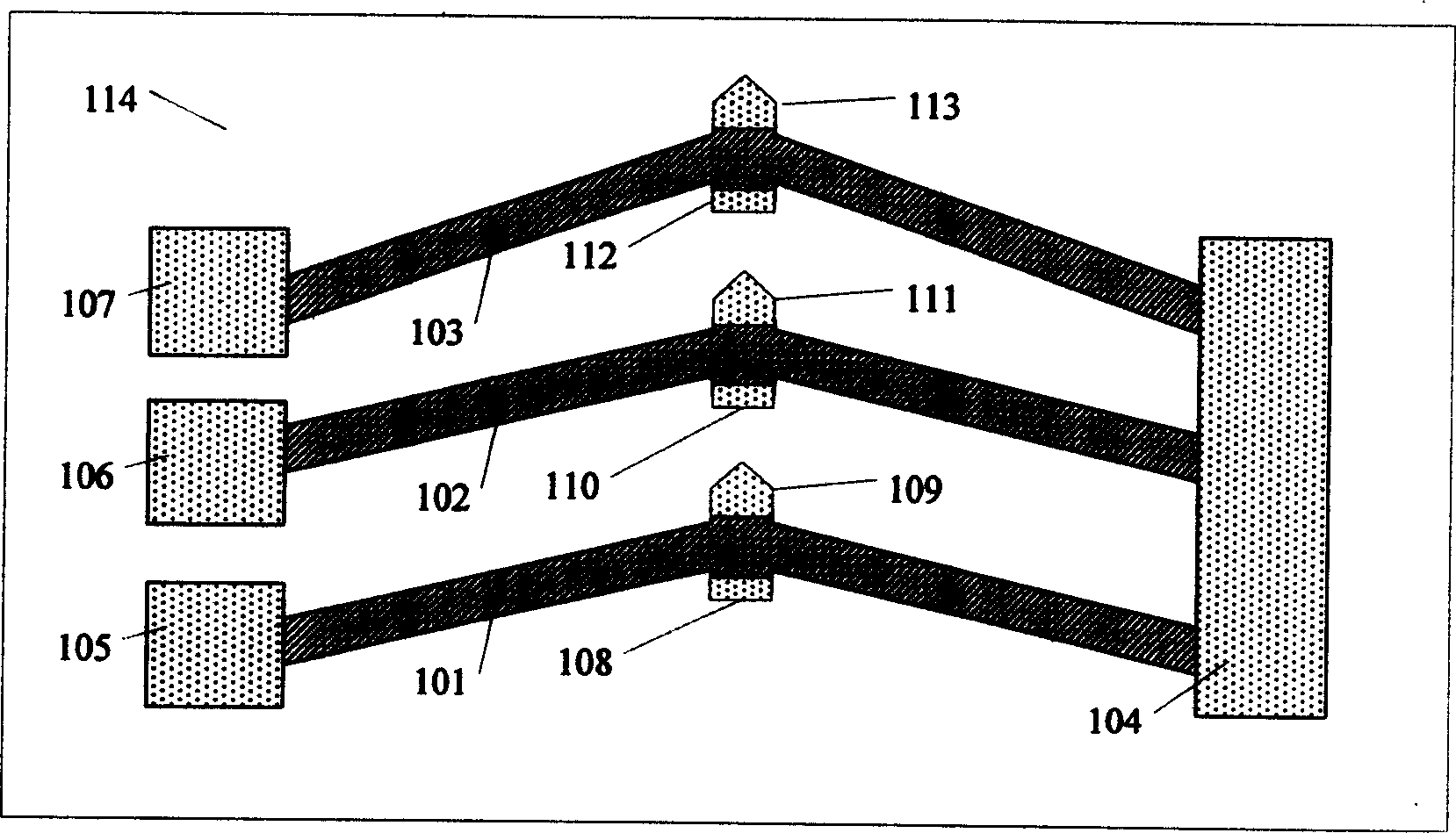
[0012] The present invention is an on-line detection structure for the residual strain of polysilicon thin films based on the surface processing technology. The soldering blocks are the first pressure-bonding block 105, the second pressure-bonding block 106, the third pressure-bonding block 107, and the fourth pressure-bonding block 104; the three polysilicon bending beams are arranged in parallel, in the middle of the three polysilicon bending beams Contacts are respectively provided on both sides of the point, and the distance between the contacts is equal; The second pressure welding block 106 and the fourth pressure welding block 104 are respectively connected, and the two ends of the third curved beam 103 are respectively connected with the third pressure welding block 107 and the fourth pressure welding block 104 . In order to make the adjacent curved beam structures have better electrical contact, the middle of each curved beam is plated with a metal film, that is, the ...


PUM


Abstract

The invention is the online detecting structure and method of polysilicon film residue deformation. The detecting structure comprises the first curved girder, the second curved girder, the third curved girder, the primary pressure welding block, the second pressure welding block, the third pressure welding block and the fourth pressure welding block. The three polysilicon curved girders parallel with each other; the contactors are at the two sides of the central point of the girders and the space between the contactors is equal. The two ends of the first curved girder separately connect the primary and the forth pressure welding blocks; the two ends of the second girder separately connect the second and the forth pressure welding blocks; the two ends of the third girder connect the third and the forth pressure welding blocks. The invention has fast detecting speed and low requirement for the detected equipment.

Description

technical field [0001] The invention relates to an on-line detection structure for residual strain of polysilicon thin films based on a surface processing technology, and belongs to the technical field of micro-electromechanical system (MEMS) process parameter testing. Background technique [0002] Polysilicon is a very important material in both the integrated circuit (IC) industry and in the Micro Electro Mechanical System (MEMS), and has been successfully used to fabricate micro-mechanical structures, integrated electrical interconnects, thermocouples, p-n junction diodes and other electronic devices with micromechanical structures. Polysilicon-based surface processing technology has now become an important thin and flat device fabrication technology. The research on the material parameters of polysilicon thin film has been started from the early stage of the development of integrated circuits, but the previous research on polysilicon thin film focused more on its prepar...

Claims


Application Information

Patent Timeline
Patent Type & Authority Applications(China)
IPC IPC(8): G01B7/16
Inventor 黄庆安刘祖韬李伟华
Owner SOUTHEAST UNIV
Learn More