

Contact probe, method of manufacturing the contact probe, and device and method for inspection
A technology for inspection devices and probes, applied to measuring devices, instruments, measuring electronics, etc., can solve problems such as increased contact area
- Summary
- Abstract
- Description
- Claims
- Application Information
AI Technical Summary
Problems solved by technology
Method used
Image

Examples
Embodiment 1
[0071] refer to Figure 1-9 A method of manufacturing a contact probe according to Embodiment 1 of the first aspect of the present invention will be described.
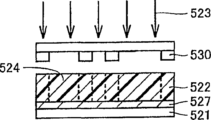
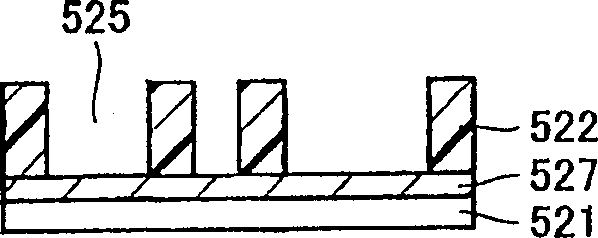
[0072] First, a resist film 522 is formed on a conductive substrate 521 . A metal substrate such as SUS, Cu, Al, or the like, a Si substrate, a glass substrate, or the like can be used as the substrate 521 . Among them, in the case of a Si substrate, a glass substrate, etc., a metal layer of Ti, Al, Cu, Ni, Mo or their alloys should be formed on the substrate 521 by sputtering in advance, and used as the base conductive layer 527. . Furthermore, even when a metal substrate is used, if necessary, the base conductive layer can be formed on the metal substrate by sputtering. Hereinafter, the case where the base conductive layer 527 is provided will be described with reference to the drawings.
[0073] Such as figure 1 As shown, using a mask 530, the surface of the resist film 522 is irradiated with X-rays 523 from ...
Embodiment 2
[0083] refer to Figure 13 ~ Figure 21 , Figure 8 , Figure 9 A method of manufacturing a contact probe according to Embodiment 2 of the first aspect of the present invention will be described.
[0084] Such as Figure 13 As shown, using a convex mold 532 having contact probes, a resin mold 533 is formed by injection molding or the like. The result is as Figure 14 As shown, a resin type 533 having a concave contact probe shape was obtained. Grinding the resin type 533 through the recess, made as Figure 15 The resin graphic box 534 is shown. Such as Figure 16 As shown, a substrate 521 is prepared, on which a base conductive layer 527 is formed as shown in Embodiment 1, and a graphic frame 534 is pasted on the base conductive layer 527 . However, as described in the first embodiment, when the substrate 521 is a metal substrate, there is no problem even if the base conductive layer 527 is not provided. It should be noted that the resin mold 533 may be pasted on the s...
Embodiment 3
[0089] refer to Figure 1~4 , Figure 22 , Figure 23 , Figure 7 ~ Figure 9 The manufacturing method of the contact probe according to the third embodiment of the first aspect of the present invention will be described.
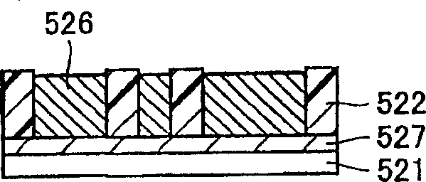
[0090] about in Figure 1 ~ Figure 4 The steps shown are the same as those described in Embodiment 1. Such as Figure 4 As shown, after the upper surface of the grinding metal layer 526 is processed to a desired thickness, in this embodiment, as Figure 22 Polishing is performed as shown to remove the resist film 522 . Then, if Figure 23 Electrical discharge machining is performed by electrical discharge machining electrode 542 as shown. The electric discharge machining electrode 542 is an electrode with a conical or V-shaped tip. By this electrical discharge machining, a portion to be the tip of the contact probe is machined to form an inclined machined surface.
[0091] exist Figure 23 In the illustrated example, the electric discharge machini...
PUM
 Abstract
Description
Claims
Application Information