Solid state image pickup device and its manufacturing method

A solid-state imaging device and solid-state image pickup technology, which are used in image communication, electrical solid-state devices, televisions, etc., can solve the problems of easy cracking of solid-state image pickup components, hindering productivity improvement, and decreasing productivity, saving manpower, Realize the effect of miniaturization and simplification of structure

Inactive Publication Date: 2005-11-09
PANASONIC CORP
View PDF2 Cites 14 Cited by
  • Summary
  • Abstract
  • Description
  • Claims
  • Application Information

AI Technical Summary

Problems solved by technology

Therefore, the problem with the conventional device is that many connections must be made during the installation of the parts, so the size of the device is large and the installation process takes a long period of time.
[0015] In various methods, due to the thermal deformation of the 3D printed circuit board, the bonding of the solid-state image pickup element is extremely prone to cracking, which will lead to a decrease in production yield
[0016] When a printed circuit board is made into a three-dimensional structure, it can be miniaturized, but its thermal deformation is generally larger than that of a two-dimensional structure, so there is a serious problem that deformation due to a difference in expansion coefficient hinders yield improvement

Method used


Image

  • Solid state image pickup device and its manufacturing method
  • Solid state image pickup device and its manufacturing method
  • Solid state image pickup device and its manufacturing method

Examples


Embodiment 1

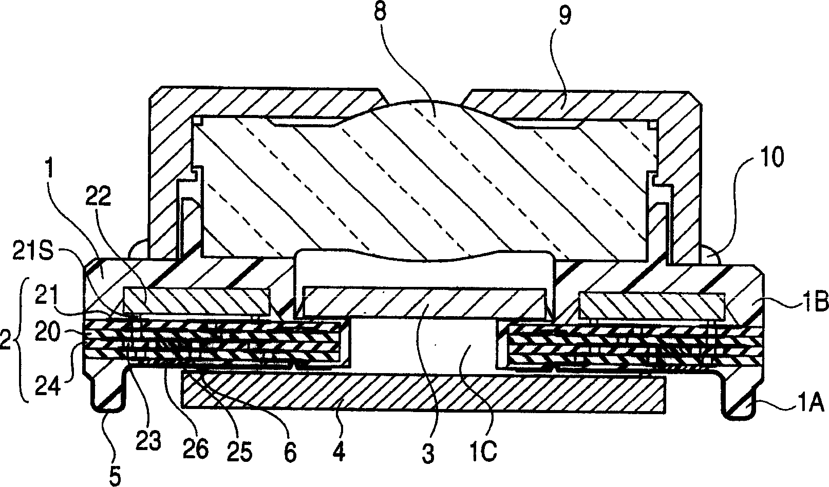
[0092] figure 1 and 2 is a view of the main body portion of the solid-state imaging device of the first embodiment of the present invention.

[0093] In this solid-state imaging device, in the molding process of the structural member 1 on which the solid-state image pickup element is mounted, the multilayer wiring board 2 and the signal processing circuit chip DSP formed on the first surface of the multilayer wiring board 2 22 are sealed together into the structure 1 made of insulating polyphthalamide resin. In addition, a multilayer wiring board is used as a service circuit board of a ceramic substrate forming a base member whose thermal expansion coefficient is significantly smaller than that of a resin constituting the structural member. The structural member 1 has a through-hole portion 1C. The plate-shaped member constituting the optical filter 3 is mounted to the structural member 1 including the processing circuit chip DSP 22 therein so as to face the through-hole p...

Embodiment 2

[0115] Figure 4 is a view of a main body portion of a solid-state imaging device according to a second embodiment of the present invention.

[0116] In the first embodiment, the optical filter 3 is mounted to a multilayer wiring board. In contrast, in the second embodiment, the ceramic substrate constituting the multilayer wiring board is made of light-transmitting ceramics, and a required thin film is formed on the surface as the polyrefringence material 20S used as an optical filter. The multilayer wiring board sealed into the structural member is constructed in the following manner. A polyrefringence material 20S is used as an insulating base, and the multilayer wiring structure 2M is formed so as to have a ring shape in a peripheral area except for a corresponding area to the through-hole portion 1C. The multilayer wiring structure 2M is placed in an injection mold, and then injection molded to seal the central region of the multilayer wiring structure 2M with a structu...

Embodiment 3

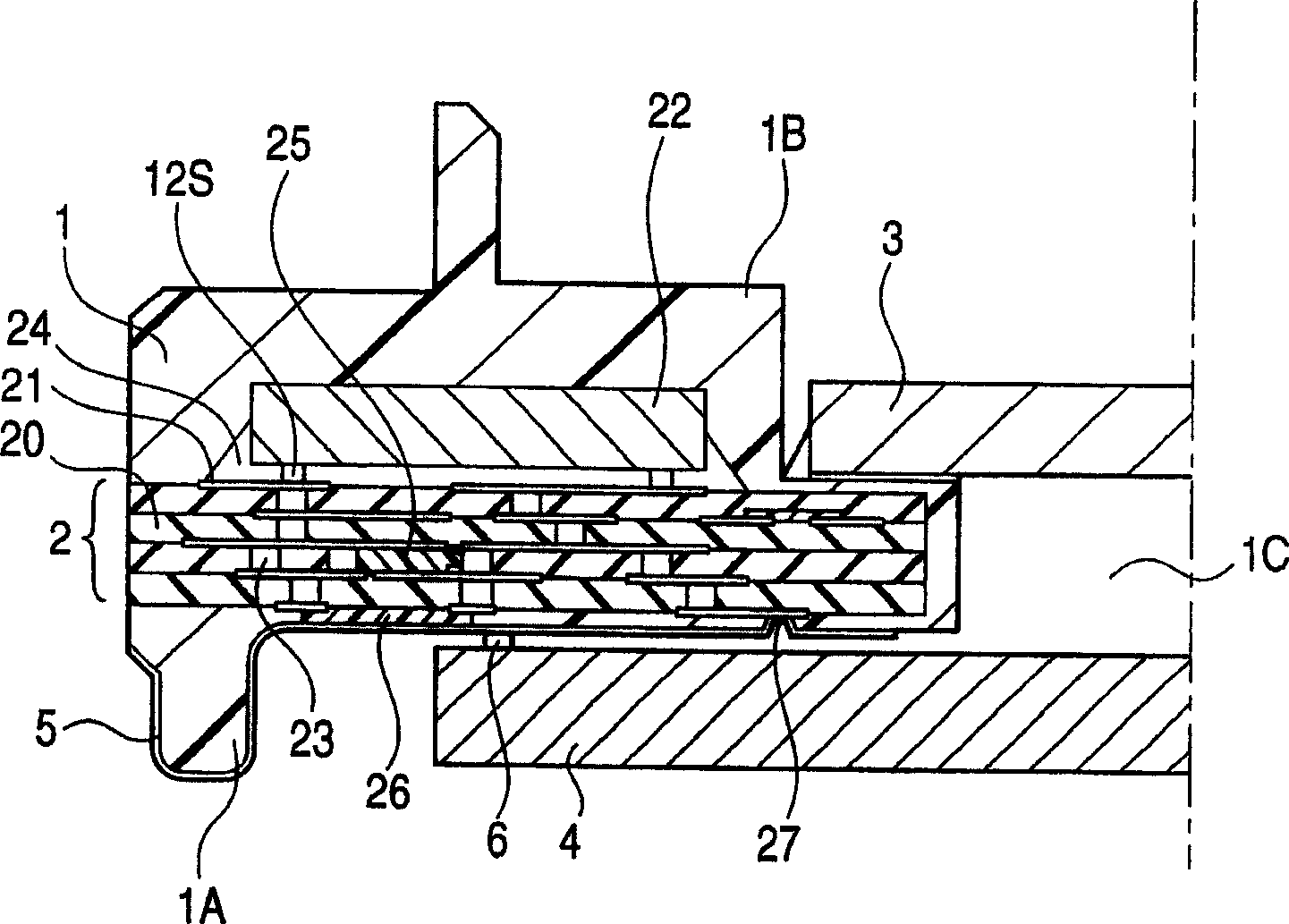
[0121] Figure 6 and 7 is a view of a main body portion of a solid-state imaging device according to a third embodiment of the present invention. Figure 7 is along Figure 6 A cross-sectional view taken along the line A-A.

[0122] In this solid-state imaging device, in the molding process of the structural member 101 on which the solid-state image pickup element 104 is mounted, the ceramic substrate 102g and the circuit part 102 of the multilayer structure formed on the film carrier 120F used as a flexible substrate are separated from the The signal processing circuit chip (DSP) 122 formed on the first surface of the ceramic substrate 102g is sealed together with the insulating polyphthalamide resin through the through hole (not shown) opened on the ceramic substrate 102g. In the structural member 101. In addition, a ceramic substrate 102g is used as a fixing member, and the coefficient of thermal expansion of the ceramic substrate 102g is remarkably smaller than that of...


PUM


Abstract

A structure member is used wherein a circuit board is connected to a solid-state image pickup element and placed between a portion of the structure member to which the solid-state image pickup element is attached, and another portion to which a light-transmitting member is attached, and the circuit board is sealed integrally into the structure member. The solid-state image pickup element is attached to a through-opening portion 1 C, and a light-transmitting member is attached so as to cover the through-opening portion 1 C with being separated from the solid-state image pickup element by a predetermined distance. In a process of molding the structure member, the circuit board is integrally molded, whereby the manpower can be reduced, and the structures of the attaching portions can be simplified to miniaturize the device.

Description

[0001] This application is a divisional application of an invention patent application titled "Solid State Imaging Device and Its Manufacturing Method", application number 02151570.0, filing date November 30, 2002, and applicant Matsushita Electric Industrial Co., Ltd. technical field [0002] The present invention relates to a solid-state imaging device and a manufacturing method thereof, and more particularly to a compact imaging device having a solid-state image pickup element such as a surveillance camera, a medical camera, or a vehicle-mounted camera and a manufacturing method thereof. Background technique [0003] Such an imaging device receives an image through an optical system such as a lens, and outputs the image in the form of an electric signal. In recent years, with the miniaturization and improvement in performance of such imaging devices, and the decreasing size of image pickup devices, imaging devices are used in various fields and their market is expanding to...

Claims


Application Information

Patent Timeline
IPC IPC(8): H01L27/14H04N1/028H04N5/225H04N5/335
Inventor 原园文一
Owner PANASONIC CORP
Why Eureka
Try Eureka