Wave-guide integrated on substrate-electronic band gap band pass filter

A substrate-integrated waveguide and electronic bandgap technology, which is applied to waveguide-type devices, waveguides, circuits, etc., can solve the problems of bulky band-pass filters, high processing precision, and expensive processing of band-pass filters. The method is simple, the frequency selection characteristic is increased, and the volume is reduced.

Inactive Publication Date: 2005-11-16
SOUTHEAST UNIV
View PDF0 Cites 9 Cited by
  • Summary
  • Abstract
  • Description
  • Claims
  • Application Information

AI Technical Summary

Problems solved by technology

However, it is difficult for these forms of filters to achieve a very wide relative bandwidth (≥50%). Secondly, these forms of bandpass filters are relatively bulky and difficult to integrate with oth

Method used


Image

  • Wave-guide integrated on substrate-electronic band gap band pass filter
  • Wave-guide integrated on substrate-electronic band gap band pass filter
  • Wave-guide integrated on substrate-electronic band gap band pass filter

Examples


Embodiment Construction

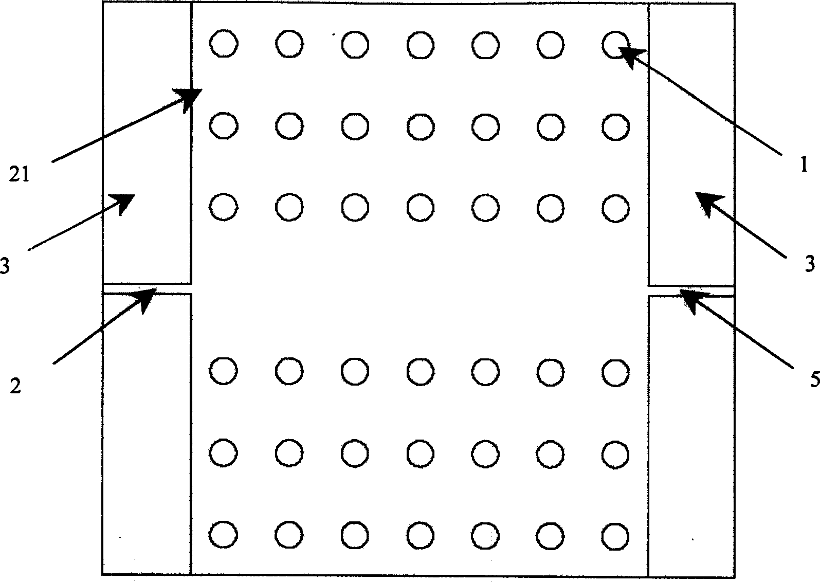
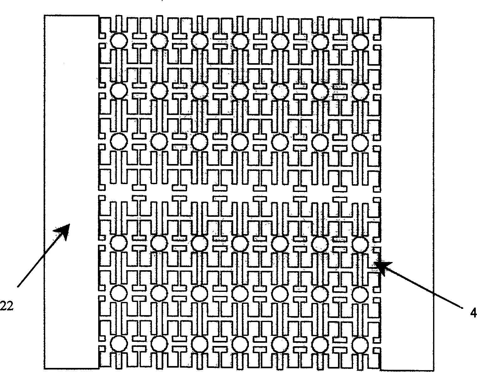
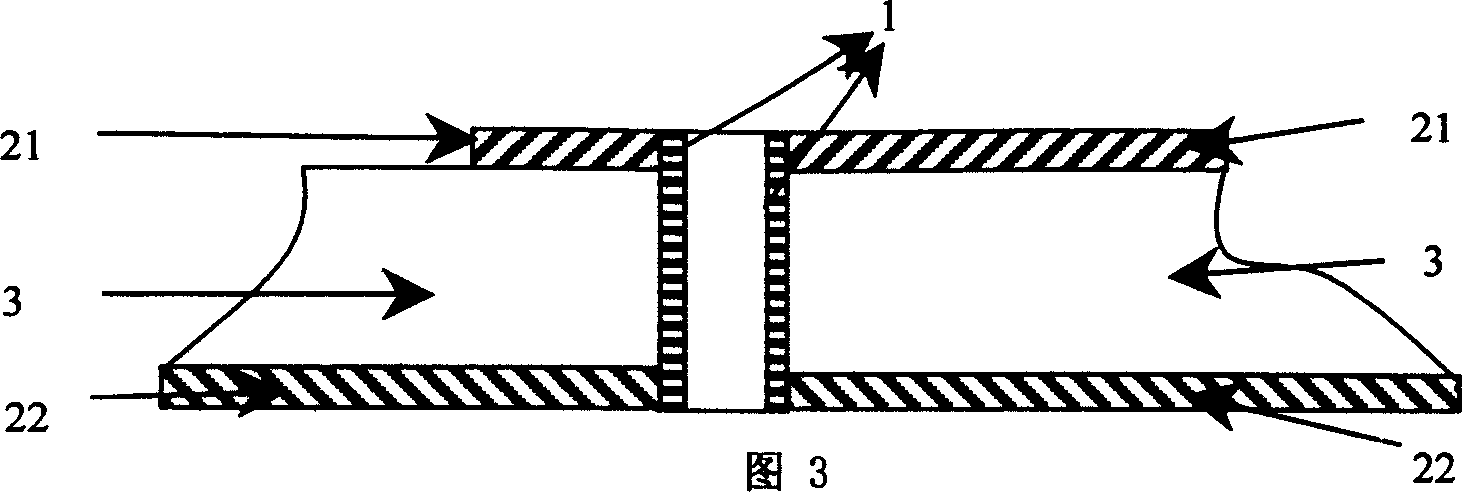
[0017] A substrate-integrated waveguide-electronic bandgap bandpass filter, comprising: a dielectric substrate 3 covered with metal patches 21 and 22 as the top surface and the ground respectively on both sides, and the dielectric substrate 3 is provided with a substrate Chip integrated waveguide, the substrate integrated waveguide is composed of at least 2 rows of metallized through holes 1, the metal patches 21 and 22 are connected by metallized through holes 1, and an electronic bandgap structure is arranged on the ground of the dielectric substrate 3. The top surface of the dielectric substrate 3 is provided with an input terminal 2 and an output terminal 5 and is respectively connected to the integrated waveguide of the same substrate. The electronic bandgap structure is composed of coplanar compact electronic bandgap units 4 arranged in an array, and at least 1 The coplanar compact electronic bandgap unit is located on the ground of the inner area of ​​the substrate integ...


PUM


Abstract

The disclosed filter includes a medium base plate. Metal pasters covered on both sides of the said base plate are as a top surface and floor. Substrate integration wave-guide (SIW) on base plate is setup at the medium base plate, and electronic band gap is setup at floor. Input end and output end are connected to integrated wave-guide on same base plate respectively. Structure of electronic band gap is composed of compact type units of electronic band gap arranged in array in same plane. Advantages are: small size of integrated structure of electronic band gap with SIW in filter, easy to be integrated with other ICs, wide frequency selectivity, simple designing method, and possible to add number of identical unit of structure of electronic band gap to increase frequency selectivity.

Description

technical field [0001] The invention relates to a substrate integrated waveguide that can be applied to the design of microwave and millimeter wave circuits, and can also be used in the design of microwave and millimeter wave integrated circuits in highly integrated systems such as system package (SOP) and system on chip (SOC) -- electronic bandgap bandpass filter. Background technique [0002] Microwave and millimeter wave bandpass filters have a large number of applications in rapidly developing communication systems. With the rapid development of broadband communication systems, there is an urgent need for filters with very wide passbands. Broadband microwave and millimeter wave bandpass filters can be formed using traditional structures such as metal ridge waveguides. However, it is difficult for these forms of filters to achieve a very wide relative bandwidth (≥50%). Secondly, these forms of bandpass filters are relatively bulky and difficult ...

Claims


Application Information

Patent Timeline
IPC IPC(8): H01P1/201
CPCH01P1/2005
Inventor 洪伟郝张成陈继新吴柯
Owner SOUTHEAST UNIV
Why Eureka
Try Eureka