CMOS image sensor, reset transistor control circuit and voltage switch circuit

An image sensor and control circuit technology, applied in image communication, radiation control devices, televisions, etc., can solve problems such as the limited value of ON resistance, and achieve the effect of reducing reset noise and reducing noise components

Inactive Publication Date: 2006-01-04
FUJITSU MICROELECTRONICS LTD
View PDF1 Cites 6 Cited by
  • Summary
  • Abstract
  • Description
  • Claims
  • Application Information

AI Technical Summary

Problems solved by technology

[0004] However, when the CMOS switching element is shorted to the reset level, the ON resistance of the element is a finite value

Method used


Image

  • CMOS image sensor, reset transistor control circuit and voltage switch circuit
  • CMOS image sensor, reset transistor control circuit and voltage switch circuit
  • CMOS image sensor, reset transistor control circuit and voltage switch circuit

Examples


Embodiment Construction

[0019] The present invention is explained in detail below with reference to preferred embodiments and drawings. In the drawings, like reference numerals denote like elements.

[0020] [First preferred embodiment]

[0021] Before explaining the CMOS image sensor of the present invention, the CMOS image sensor described in Patent Document 1 is first explained.

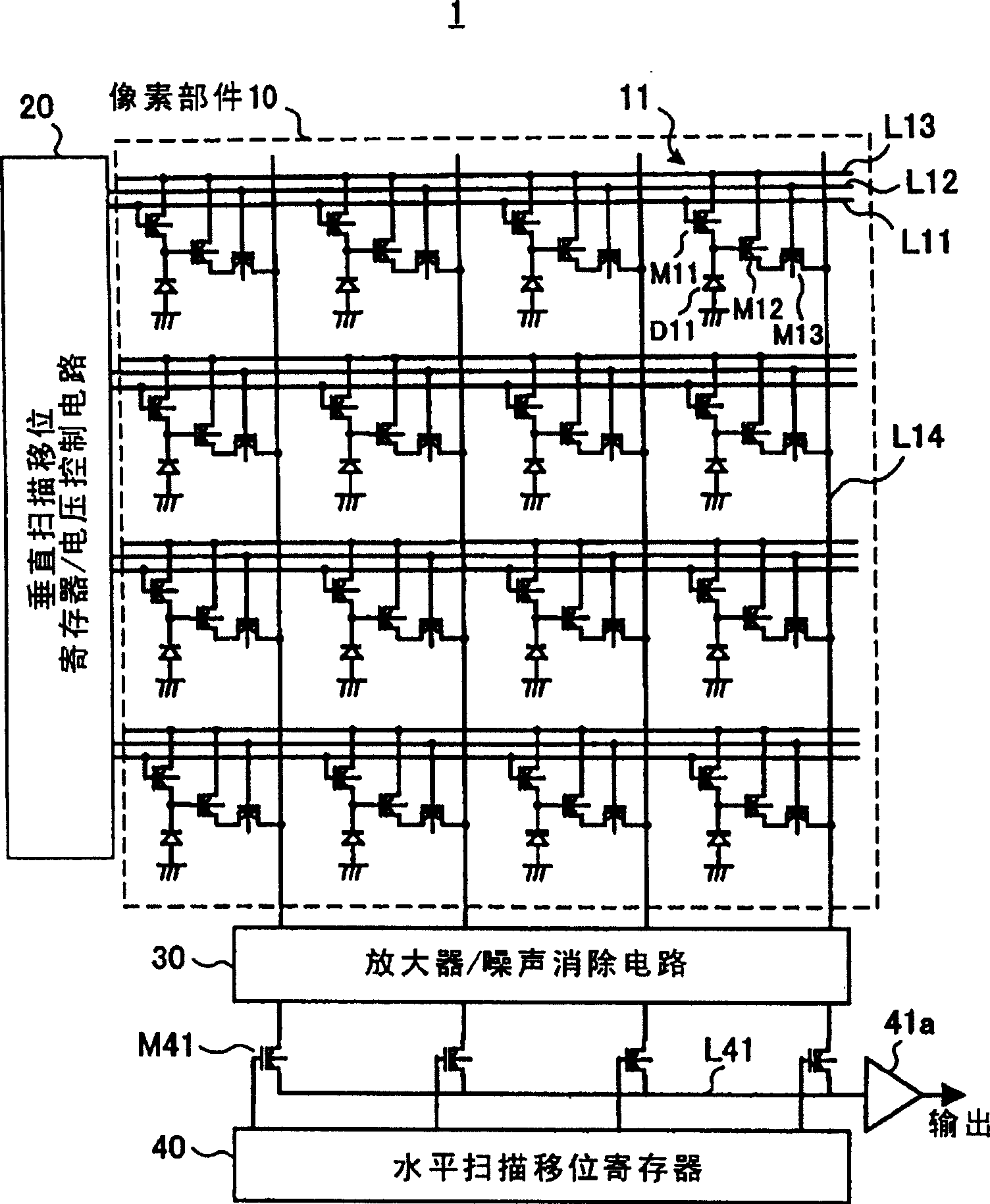
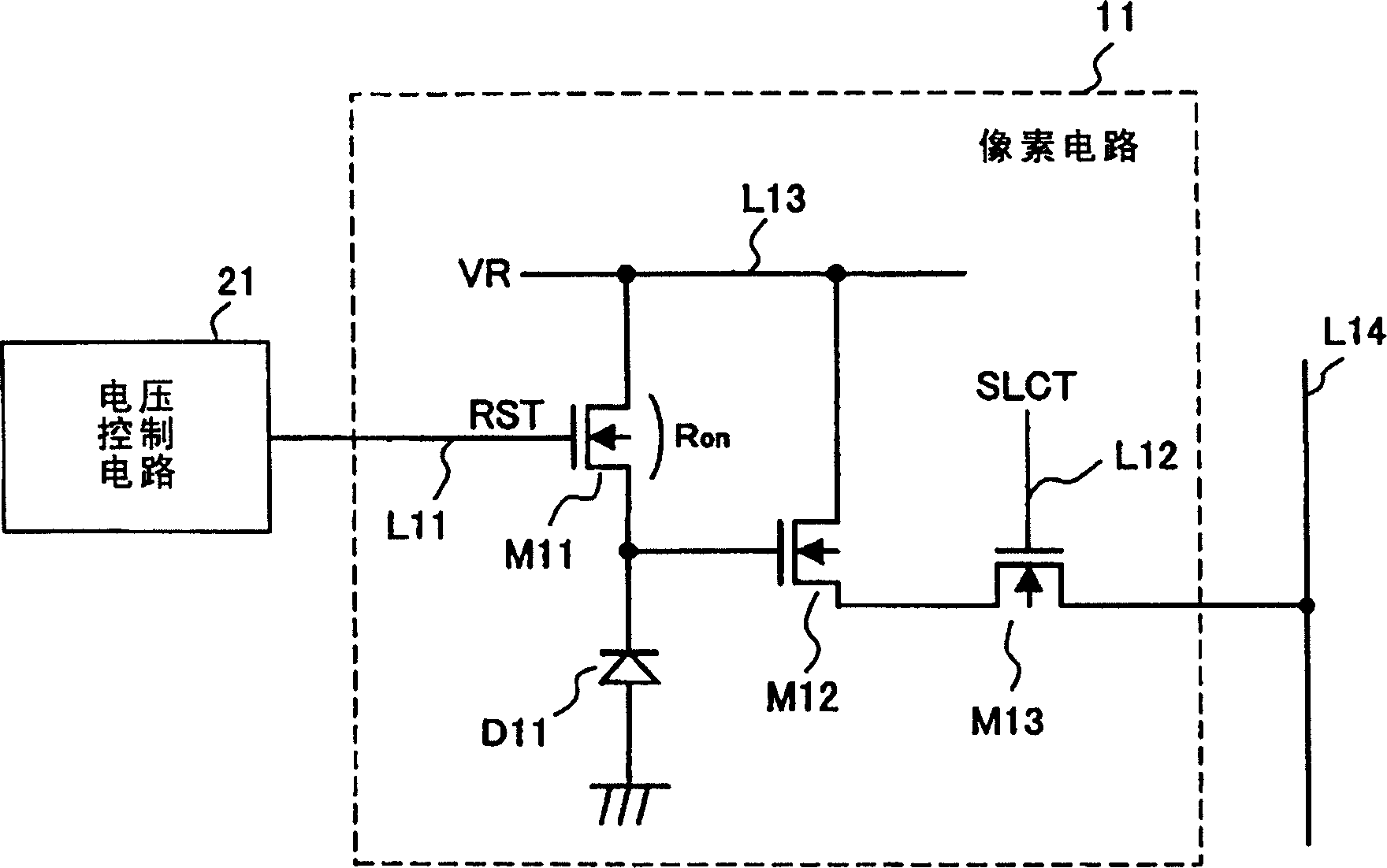
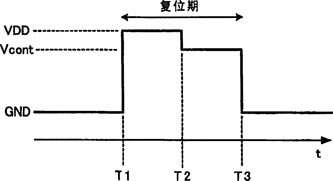
[0022] Figure 1A to Figure 1C An outline of the CMOS image sensor of Patent Document 1 is shown. Figure 1A is an overall view of the CMOS image sensor 1 . Figure 1B is a circuit diagram showing the pixel circuit 11 and the voltage control circuit 21 for supplying the control voltage (ie, gate voltage) RST of the CMOS switching element M11 of the pixel circuit 11 . Figure 1C is a waveform diagram showing the waveform of the control voltage RST.

[0023] exist Figure 1A Among them, a CMOS image sensor includes pixel elements 10 arranged in a matrix.

[0024] like Figure 1B As shown, each pixel circuit 11 includ...


PUM


Abstract

The invention can be applicable to a CMOS image sensor. In the CMOS image sensor, every pixel circuit of an active pixel sensor array includes a photoelectric transition element which is used for transiting input lights into electricity and a switching transistor which is used for controlling the reduction voltage supply to the photoelectric transition element. The reduction voltage is used for resetting the photoelectric transition element to the predetermined voltage. The CMOS image sensor includes a control circuit which is used for distributing control signals that are applied on the control electrode of the switching transistor. In the first part of the reduction period of the photoelectric transition element, the control circuit outputs first voltage which is higher than the power voltage of the CMOS image sensor to change the ON resistance of the switching transistor to be as small as possible. And in the back part of the reduction period of the photoelectric transition element, the control circuit outputs second voltage which is lower than the power voltage of the CMOS image sensor.

Description

technical field [0001] The present invention relates generally to CMOS image sensors, and more particularly to a voltage control circuit and a voltage switching circuit for use in the voltage control circuit, the voltage control circuit generating a control voltage for a switching element for controlling a pair of A reset voltage supply for a photoelectric conversion element of each pixel circuit in a CMOS image sensor. Background technique [0002] A CMOS (Complementary Metal Oxide Semiconductor) image sensor includes a pixel section in which pixel circuits for acquiring an image for one pixel are arranged in a matrix, and the output of each pixel circuit is sequentially selected by using a vertical and horizontal scanning shift register. An image signal for one page is output. In each pixel circuit, after a photoelectric conversion element such as a photodiode is short-circuited at a predetermined reset voltage every time an image is acquired, the charging voltage of the ...

Claims


Application Information

Patent Timeline
Patent Type & Authority Applications(China)
IPC IPC(8): H01L27/146H04N5/335H04N5/357H04N5/363H04N5/369H04N5/374
CPCH04N5/363H04N25/65
Inventor 柳沢诚水口寿孝井上忠夫
Owner FUJITSU MICROELECTRONICS LTD
Why Eureka
Try Eureka