Chip resistor and method of manufacturing the same

A chip resistor and resistive film technology, applied in the direction of resistors, trimming resistors, non-adjustable metal resistors, etc., can solve the problems of small change rate, long time, low retention rate, etc., and achieve weight increase and decrease, The effect of reducing manufacturing cost and reducing retention rate

Inactive Publication Date: 2006-01-04
ROHM CO LTD
View PDF2 Cites 9 Cited by
  • Summary
  • Abstract
  • Description
  • Claims
  • Application Information

AI Technical Summary

Problems solved by technology

[0012] (1) Although the two trimming grooves 9', 10' have both the number of twists and turns to increase the length of the path through which the current flows in the resistive film 5' and the two terminal electrodes 3', 4' The resistance value between them is adjusted to fall within the specific specification range, but the two trimming grooves 9', 10' are still separated by their width dimension W and the two terminals because they are arranged on the resistance film 5'. On the part where the electrodes 3', 4' are connected, the change rate of the resistance value per unit length of the two trimming grooves 9', 10' is small, so by measuring the resistance between the two terminal electrodes 3', 4' When setting the two trimming grooves 9', 10' at the same time as setting the resistance value and trimming and adjusting the resistance value to fall into a specific specification range, it takes a lot of time and the productivity is low.
[0013] (2). The resistance film 5' is formed by reducing the difference between the resistance value before the two trimming grooves 9', 10' and the resistance value after the two trimming grooves 9', 10', Therefore, when the rate of change of the resistance value per unit length of the two trimming grooves is the same in the two trimming grooves 9', 10', the retention rate of the resistance value falling within a specific specification range can be reduced. The productivity is low, which leads to the increase of manufacturing cost
[0019] In order to avoid the generation of such unqualified products, although it is sufficient to estimate the part of the positional deviation error during the engraving process and widen the interval between the two trimming grooves 30', 31', such a configuration will not only increase the length dimension of the insulating substrate 22, and will lead to an increase in size and weight

Method used


Image

  • Chip resistor and method of manufacturing the same
  • Chip resistor and method of manufacturing the same
  • Chip resistor and method of manufacturing the same

Examples


Embodiment Construction

[0048] Embodiments of the present invention will be described below with reference to the drawings.

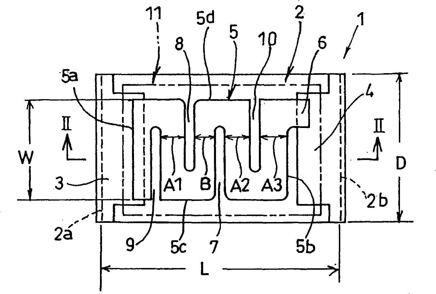
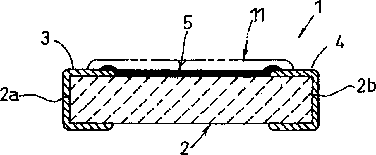
[0049] figure 1 and figure 2 The chip resistor 1 according to Embodiment 1 of the present invention is shown.

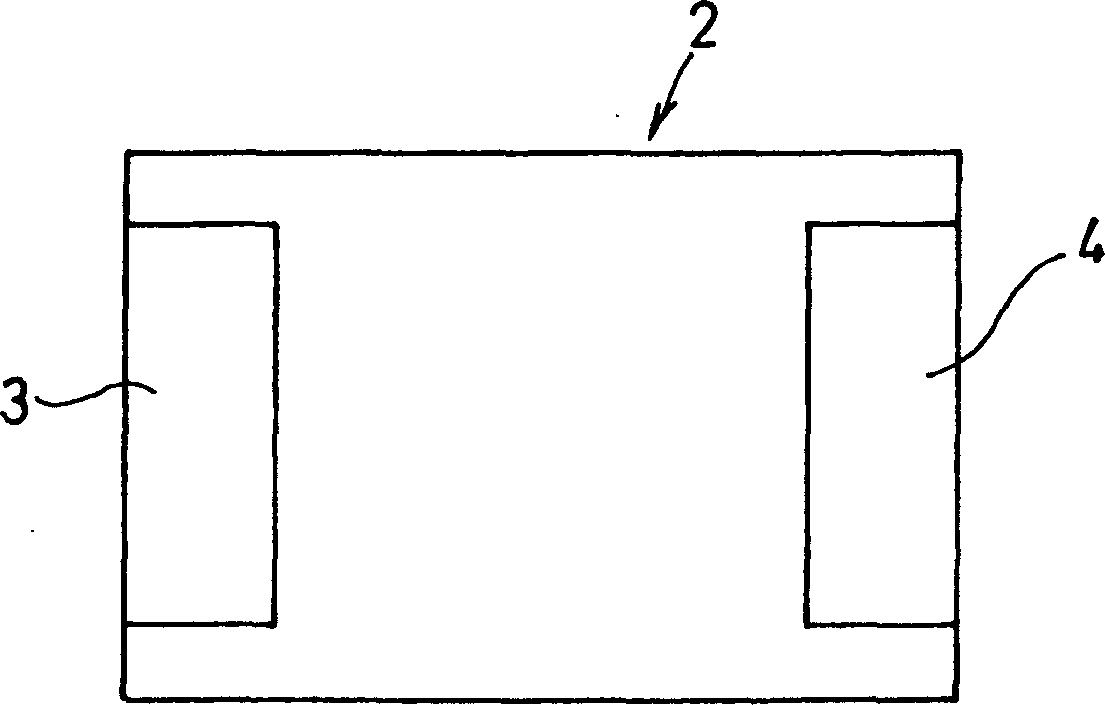
[0050] In the chip resistor 1, terminal electrodes 3 and 4 are formed on the left and right ends extending in the longitudinal direction on the upper surface of a rectangular chip-shaped insulating substrate 2 having a width D and a length L. On the one hand, on the part between the terminal electrodes 3 and 4 in the upper surface of the insulating substrate 2, the screen printing of its material paste and the subsequent calcination are used to form a suitable width dimension W along the The resistive film 5 extending in the longitudinal direction of the insulating substrate 2 .

[0051] When the resistive film 5 is formed by screen printing, one end 5a in the longitudinal direction of the resistive film 5 overlaps and connects to the one terminal electrode 3 with...


PUM


Abstract

A chip resistor, wherein a resistance film (5) is formed between a pair of terminal electrodes (2) and (3) on the upper surface of an insulating substrate (2) and two intrusion grooves (7) and (8) for making a route for passing current therethrough in a zigzag pattern and two trimming grooves (9) and (10) are alternately formed in the resistance film. The two intrusion grooves (7) and (8) are disposed adjacent to each other at a generally center part between one end (5a) and the other end (5b) of the resistance film (5), and one trimming groove (9) is formed at a portion between one intrusion groove (8) and one end (5a) of the resistance film and the other trimming groove (10) is formed at a portion between the other intrusion groove (7) and the other end (5b) of the resistance film. Thus, a time required for trimming adjustment to adjust a resistance value to a specified value can be reduced and a yielding rate can be reduced to reduce cost.

Description

technical field [0001] The present invention relates to a chip resistor having improved anti-oscillation characteristics and a manufacturing method thereof among chip resistors formed by forming a resistive film on a chip-shaped insulating substrate. Background technique [0002] In general, in a chip resistor in which a resistive film is formed on a chip-shaped insulating substrate, when an oscillating voltage is applied due to the influence of static electricity or power supply noise, the resistance value may decrease. The downside of change. It is known that the change in resistance value due to this oscillating voltage can be improved by extending the length of the path through which the current flows in the resistive film. [0003] Therefore, Patent Document 1 and Patent Document 2, which are prior art, describe chip resistors having improved oscillation resistance characteristics by having the following configuration. [0004] That is, the chip resistor 1' described ...

Claims


Application Information

Patent Timeline
IPC IPC(8): H01C17/24H01C17/06H01C7/00
Inventor 米田将记
Owner ROHM CO LTD
Why Eureka
Try Eureka