Film forming method, film forming device and storage medium

A film-forming method and technology of a film-forming device are applied in the field of reducing the size of hemispherical particles of HSG thin films, which can solve the problems of inability to form capacitors, poor step coverage of capacitive insulating films, short-circuiting of lower electrodes, etc., and achieve excellent effects. effect, improve the step coverage, suppress the effect of short circuit

Inactive Publication Date: 2006-02-15
TOKYO ELECTRON LTD
View PDF3 Cites 0 Cited by
  • Summary
  • Abstract
  • Description
  • Claims
  • Application Information

AI Technical Summary

Problems solved by technology

For example, when the diameter H1 of the annular portion of the lower electrode 4 is set at, for example, about 100 nm due to further miniaturization, or when the arrangement density of the hemispherical particles 6 is increased, the diameter D1 of the particles 6 is too large, and as a result In the subsequent process, poor step coverage of the capacity insulating film and short circuit between the lower electrodes may occur, making it impossible to make a suitable capacitor.

Method used


Image

  • Film forming method, film forming device and storage medium
  • Film forming method, film forming device and storage medium
  • Film forming method, film forming device and storage medium

Examples


Embodiment Construction

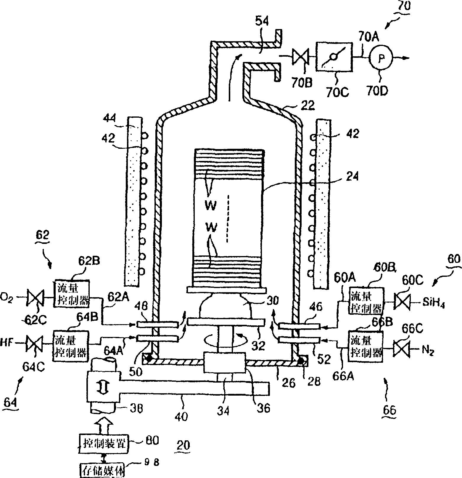
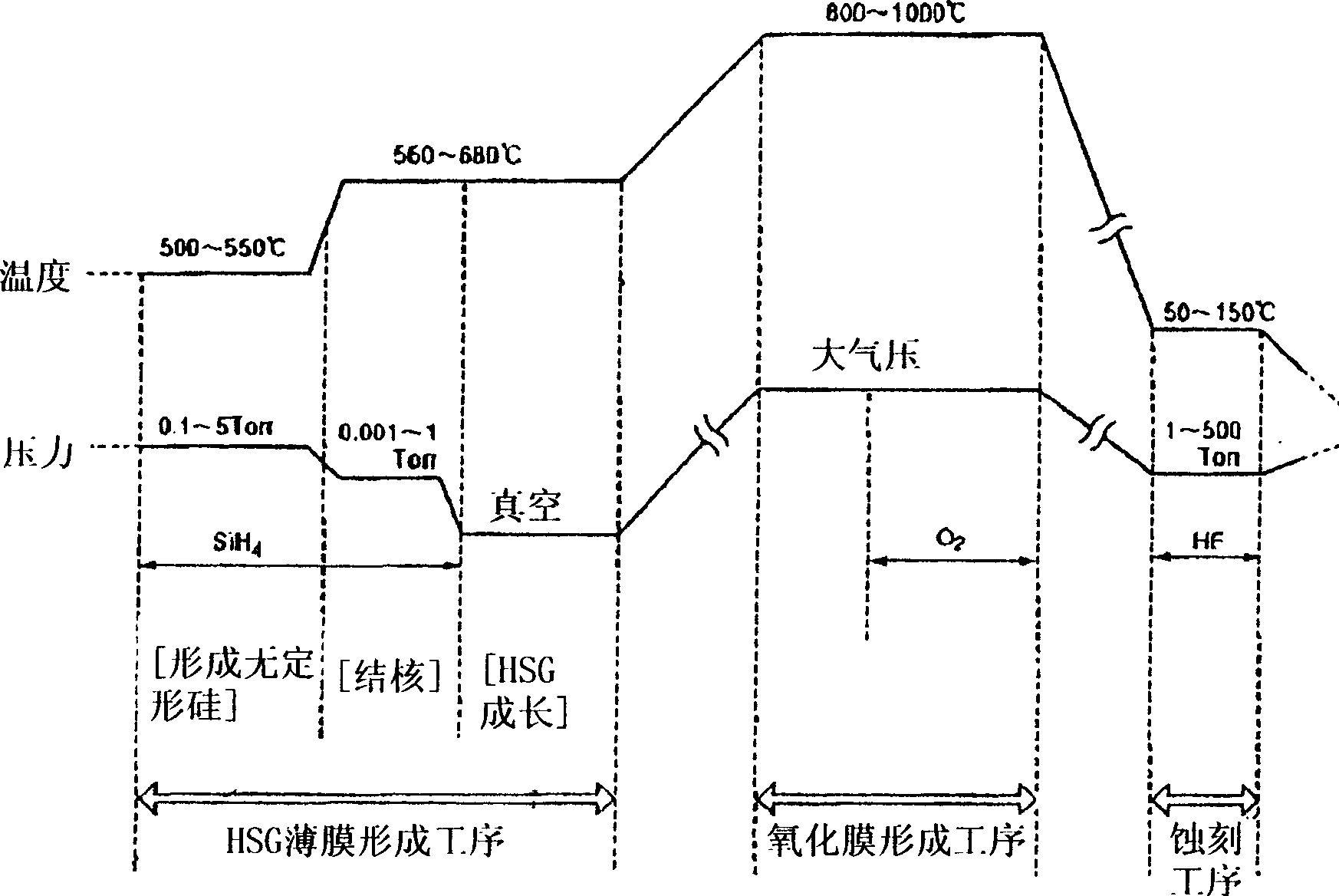
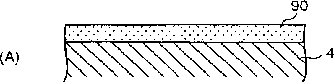
[0027] Hereinafter, an embodiment of the film forming method, film forming apparatus, and storage medium of the present invention will be described in detail based on the drawings. figure 1 is a structural diagram showing a film forming apparatus for implementing the method of the present invention, figure 2 It is a time chart representing the first embodiment flow process of the method of the present invention, image 3 It is a schematic diagram showing the formation and shape change of crystalline hemispherical particles formed by the method of the present invention.

[0028] Hereinafter, an example of an apparatus in which all of the HSG thin film forming step, oxide film forming step, and etching step can be continuously performed in this film forming apparatus will be described. As shown in the figure, the film forming apparatus 20 has a cylindrical vertical processing container 22 with an open lower end and a predetermined length in the vertical direction. The proces...


PUM


Abstract

The present invention provides a film forming method for controlling holocrystalline hemispheric granule in small size by a combination etching treatment. The film forming method of a film formed on surface of the treated object W comprises a host crystal formed on the surface of the treated object by film forming gas, the host crystal grows, the HSG film forming process one the surface of the HSG film formed by holocrystalline hemispheric granule is formed; a hemispherical grained (HSG) film is oxidized to form an oxidized layer at the surface part of the HSG film, and then the oxidized layer is etched to be removed. Thus, the film forming method controls the holocrystalline hemispheric granule in small size by a combination etching treatment.

Description

technical field [0001] The present invention relates to a film-forming method, a film-forming device, and a storage medium for forming a hemispherical grained film suitable for use as an electrode of a capacitor, and particularly relates to a technique for reducing the size of hemispherical grains of the HSG film. Background technique [0002] Generally, in order to form a semiconductor integrated circuit such as an IC, desired transistor elements are densely integrated on the surface of a semiconductor wafer, a glass substrate, etc. by repeatedly performing film formation, etching, thermal diffusion, oxidation, etc. , Resistive elements, capacitors, etc. In recent years, especially along with the high integration of semiconductor devices, the miniaturization of each element itself has been progressing. For example, in memory devices such as DRAM, as the area occupied by each unit becomes smaller, the area occupied by each cell becomes smaller and smaller. In order to ensur...

Claims


Application Information

Patent Timeline
Patent Type & Authority Applications(China)
IPC IPC(8): H01L21/3205
Inventor 长谷部一秀木村法史藤田武彦古泽纯和
Owner TOKYO ELECTRON LTD
Why Eureka
Try Eureka