LED device and method by which it is produced

a technology of led chips and manufacturing methods, applied in the direction of semiconductor/solid-state device manufacturing, semiconductor devices, electrical equipment, etc., can solve the problems of uneven heat treatment temperature needed on the exoergic member, difficult to bond multiple led chips simultaneously, uneven pressure, etc., to avoid uneven pressure application, increase brightness, and improve brightness

Inactive Publication Date: 2008-11-20
USHIO DENKI KK
View PDF4 Cites 65 Cited by
  • Summary
  • Abstract
  • Description
  • Claims
  • Application Information

AI Technical Summary

Benefits of technology

[0020]Further, in the production of the LED device of this invention, because the Au—Sn alloy layer that produces the bond is formed by alloying Sn and Au from the Sn film formed on the upper surface of the exoergic member and the Au film formed on the lower surface of the LED chip, there is no need for preparatory formation of an Au—Sn alloy, on either the exoergic member or the LED chip, in order to obtain the Au—Sn alloy layer. Besides that, the Sn film, the Au film, and the LED chip are stacked on the upper surface of the exoergic member in that order, so that the LED chip is bonded, by its own weight, to the exoergic member by way of the Au—Sn alloy layer formed by the alloying of Sn and Au, there is no need to apply pressure to the LED chip.
[0021]Accordingly, when multiple LED chips are to be bonded to the exoergic member simultaneously, it is possible to pattern the Sn layer on the upper surface of the exoergic member without inviting deterioration, and the LED chips are bonded to the exoergic member without application of pressure, with the result that deterioration caused by uneven application of pressure can be avoided.
[0022]This being the case, the LED device of this invention has a structure that allows simultaneous bonding of multiple LED chips to an exoergic member. It is possible, moreover, to increase brightness by means of a construction in which multiple LED chips are bonded to an exoergic member in this way

Problems solved by technology

It became clear that in this procedure, if an Au—Sn alloy vapor deposition layer is patterned on the upper surface of the exoergic member in order to bond multiple LED chips to a single exoergic member, variation of the composition ratio (the proportions in the construction) of the Au—Sn alloy vapor deposition layer of the patterning will occur, and so the heat treatment temper

Method used


Image

  • LED device and method by which it is produced
  • LED device and method by which it is produced
  • LED device and method by which it is produced

Examples


embodiment 1

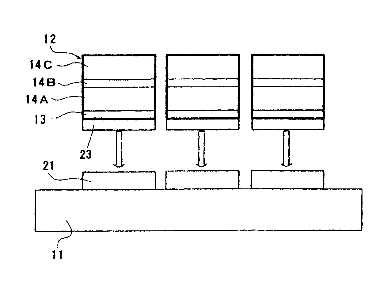
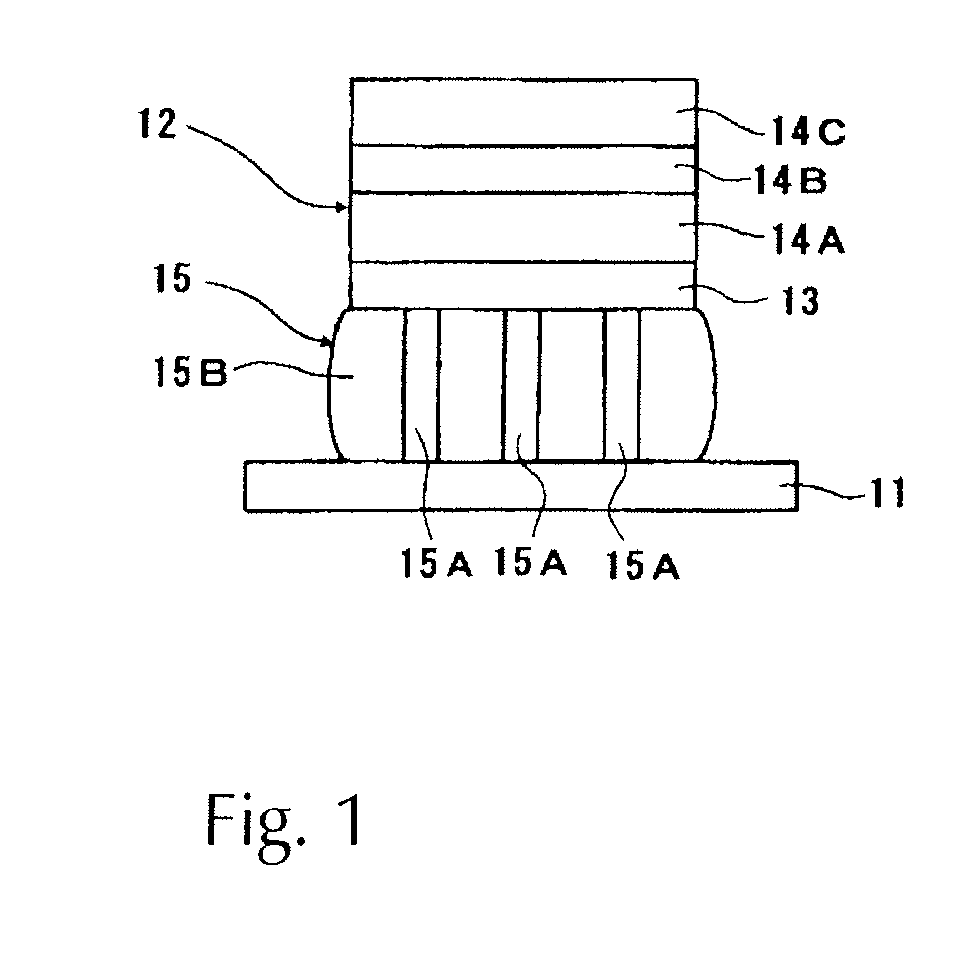
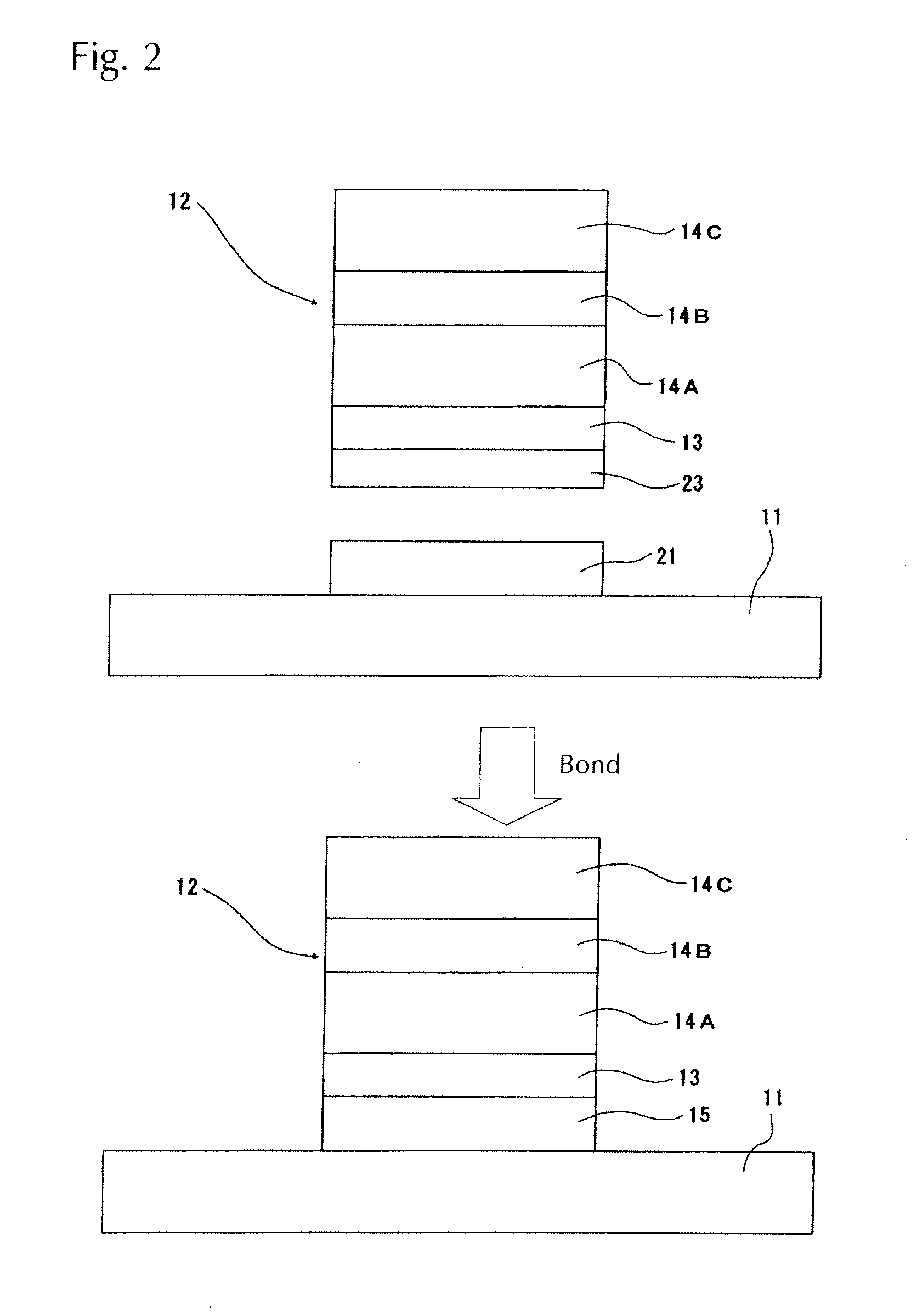
[0084]An exoergic member made of an aluminum nitride plate 5 mm long and 5 mm wide was prepared, as were 100 rectangular LED chips 350 μm long and 350 μm wide having a construction of nitride semiconductor layers which were an n-type semiconductor layer of n-GaN, a light-emitting layer of InGaN, and a p-type semiconductor layer of p-GaN, stacked in that order on sapphire substrates.

[0085]First, an Au film with a film thickness of 0.2 μm was formed by EB vapor deposition on the lower surface of the sapphire substrate of each of the 100 LED chips.

[0086]Further, an Sn film with a film thickness of 3 μm was patterned by EB vapor deposition onto each of 100 LED chip bonding regions on the exoergic member to match the lower surfaces of the LED chips to be bonded, arranged in a lattice shape of ten units vertically by ten units horizontally, separated by gaps of 30 μm.

[0087]Next, the LED chips with an Au film formed on their lower surfaces were mounted on the multiple Sn films formed on th...


PUM


Abstract

A LED device formed of LED chips bonded to an exoergic member by the LED chips being bonded to an Au—Sn alloy layer formed on an upper surface of the exoergic member with columnar crystals being formed within the Au—Sn alloy layer extending in a direction perpendicular to the upper surface of the exoergic member. The method of producing the LED device forms an Sn film directly on the upper surface of the exoergic member, an Au film on a lower surface of the LED chips, mounts the LED chips with the Au film thereon onto the Sn film formed on the upper surface of the exoergic member, and the exoergic member with LED chips mounted thereon is heated in an atmosphere in which a forming gas flows, so that the LED chips are bonded to the exoergic member.

Description

BACKGROUND OF THE INVENTION[0001]1. Field of Invention[0002]This invention concerns an LED device and a method by which it is produced. More specifically, it concerns an LED device used as a light source in display equipment, lighting equipment, and so on, and its method of production.[0003]2. Description of Related Art[0004]LED devices formed by bonding LED chips to exoergic members have been used as light sources in display equipment, lighting equipment, and so on in recent years; in these LED devices, a silicon resin or other resin is commonly used as a bonding material to bond the LED chips to exoergic members made of aluminum nitride (AlN), silicon carbide (SiC), Copper (Cu), or aluminum (Al), for example, or to lighting fixtures that function as exoergic members.[0005]There is the problem, however, that because the resin used as a bonding material that forms the bonds between the LED chips and the exoergic members have inadequate heat resistance, a heat-resistance temperature ...

Claims


Application Information

Patent Timeline
IPC IPC(8): H01L33/00H01L33/32H01L33/48H01L33/62H01L33/64
CPCH01L25/0753H01L33/641H01L2224/29144H01L2924/0105H01L2924/01079H01L2924/01322
Inventor IMAI, YUJI
Owner USHIO DENKI KK
Why Eureka
Try Eureka