

Organic electroluminescent device and method for fabricating the same
一种电致发光器件、有机的技术,应用在电致发光光源、有机半导体器件、半导体/固态器件制造等方向,能够解决降低色彩纯度和亮度等问题
Inactive Publication Date: 2006-03-22
LG DISPLAY CO LTD
View PDF0 Cites 5 Cited by
- Summary
- Abstract
- Description
- Claims
- Application Information
AI Technical Summary
Problems solved by technology
[0008] Electron-hole pairs generated in areas other than the light-emitting area only emit light in this area, so there is a problem of reducing color purity and brightness
Method used
View moreImage
Smart ImageViewing Examples

Examples
Embodiment
[0045] The ITO glass was patterned to have a size of 2 mm x 2 mm. The patterned ITO glass is then cleaned.
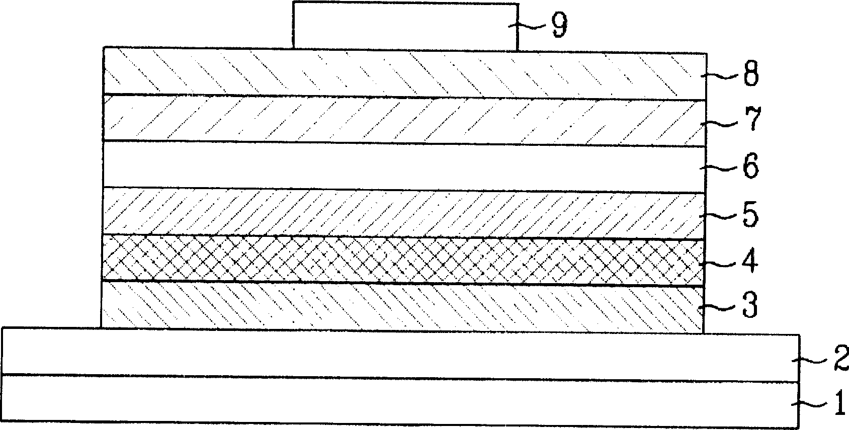
[0046] The substrate is loaded and the base pressure is set to 1 x 10 -6 Torr vacuum chamber and CuPC (200 Å), NPD (400 Å), CBP+(btp) 2 lr(acac) (8%) (200 Å), hole blocking layer (100 Å), Alq 3 (300 Å), LiF (5 Å), and Al (1000 Å) were deposited on the ITO in sequence.
[0047] When B-60 is used as the hole blocking layer, it shows 1135cd / m at about 1mA 2 (9.30V), the brightness display is about 3.2cd / A, wherein, CIE is x=0.661, y=0.328.
Login to View More PUM
| Property | Measurement | Unit |
|---|---|---|
| luminance | aaaaa | aaaaa |
Abstract
Disclosed are an organic electroluminescent device and a method for fabricating the same. The device includes a substrate, a first electrode formed on the substrate, an emission layer formed over the first electrode, and having a first emission area, a second emission area, and a third emission area, a hole blocking layer formed on the emission layer, the hole blocking layer being formed of the same substance as that of the third emission area, and a second electrode formed over the hole blocking layer.
Description
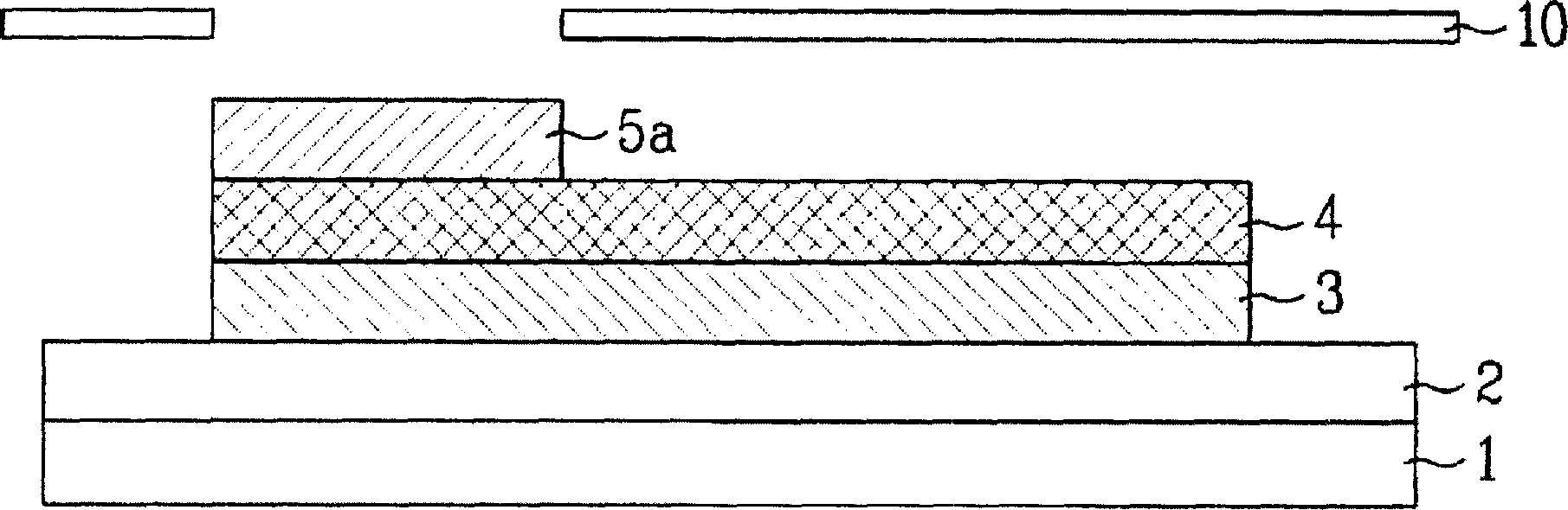
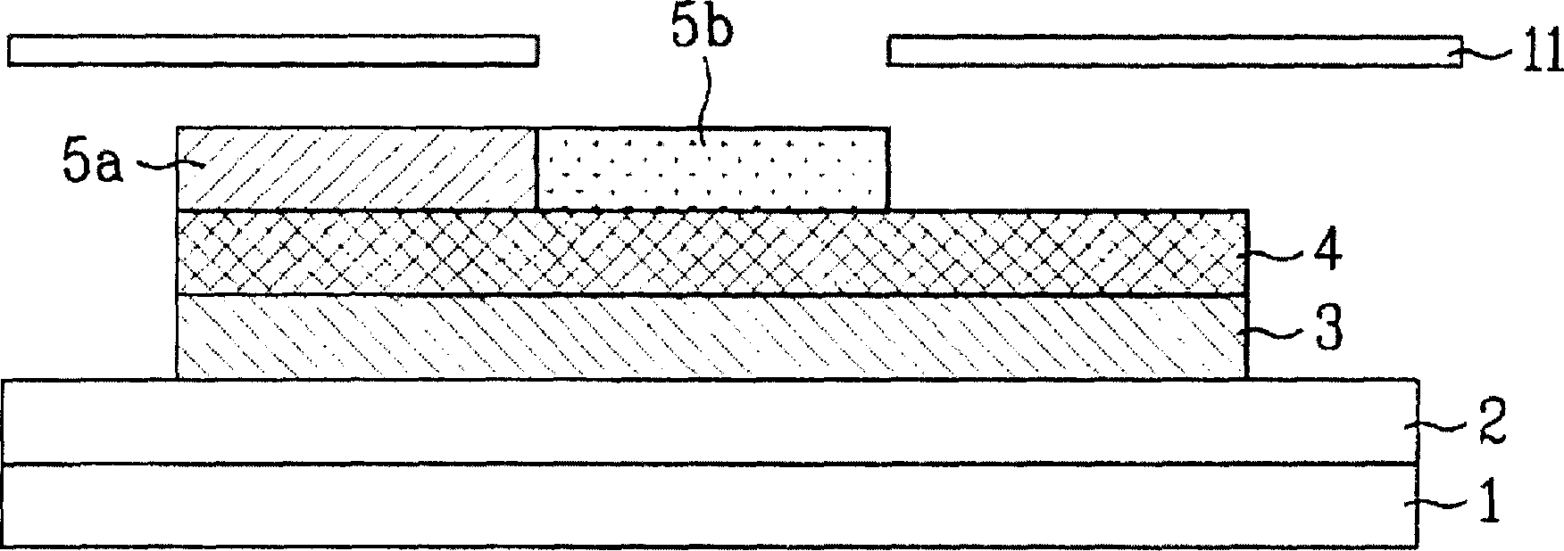
technical field [0001] The present invention relates to an organic electroluminescent device, and more particularly to an organic electroluminescent device with a hole blocking layer and a manufacturing method thereof. Background technique [0002] Recently, with the trend of large-sized displays, demand for flat panel display devices that occupy less space is increasing. Examples of flat panel displays are organic electroluminescent devices, also known as organic light emitting diodes (OLEDs). Meanwhile, organic electroluminescence display technology is rapidly developing, so various prototypes have entered the market. [0003] An organic electroluminescent device is a light-emitting device whereby charges are injected into the organic layer between the anode and cathode to form a pair of electrons and holes that create electron-hole pairs that fall back from the excited state to the ground state thereby emit light. [0004] An advantage of an organic electroluminescent ...
Claims
Login to View More Application Information
Patent Timeline
 Patent Type & AuthorityApplications(China)
IPC IPC(8): H01L51/10H05B33/10H05B33/14C09K11/06C07C15/28H05BH05B33/12H10K99/00
CPCH01L51/52H01L51/0059H01L51/0067H01L51/0052H01L51/5036H01L51/006H01L51/0085H01L2251/308H01L51/5096H01L51/0072H01L51/0081Y10S428/917H10K85/633H10K85/615H10K85/631H10K85/654H10K85/324H10K85/342H10K85/6572H10K50/125H10K50/18H10K50/80H10K2102/103C09K11/06
Inventor徐正大金憘廷李敬勋吴炯润金明燮朴春键
OwnerLG DISPLAY CO LTD