Shift register circuit

A shift register circuit, shift register technology, applied in static memory, digital memory information, instruments, etc., can solve problems such as incorrect output of displayed images and inability to fully maintain output signals

Active Publication Date: 2006-05-03
AU OPTRONICS CORP
View PDF0 Cites 22 Cited by
  • Summary
  • Abstract
  • Description
  • Claims
  • Application Information

AI Technical Summary

Problems solved by technology

It can be found from the curve 32 that after a long time of use of the existing shift register, the output signal cannot b

Method used


Image

  • Shift register circuit
  • Shift register circuit
  • Shift register circuit

Examples


Embodiment Construction

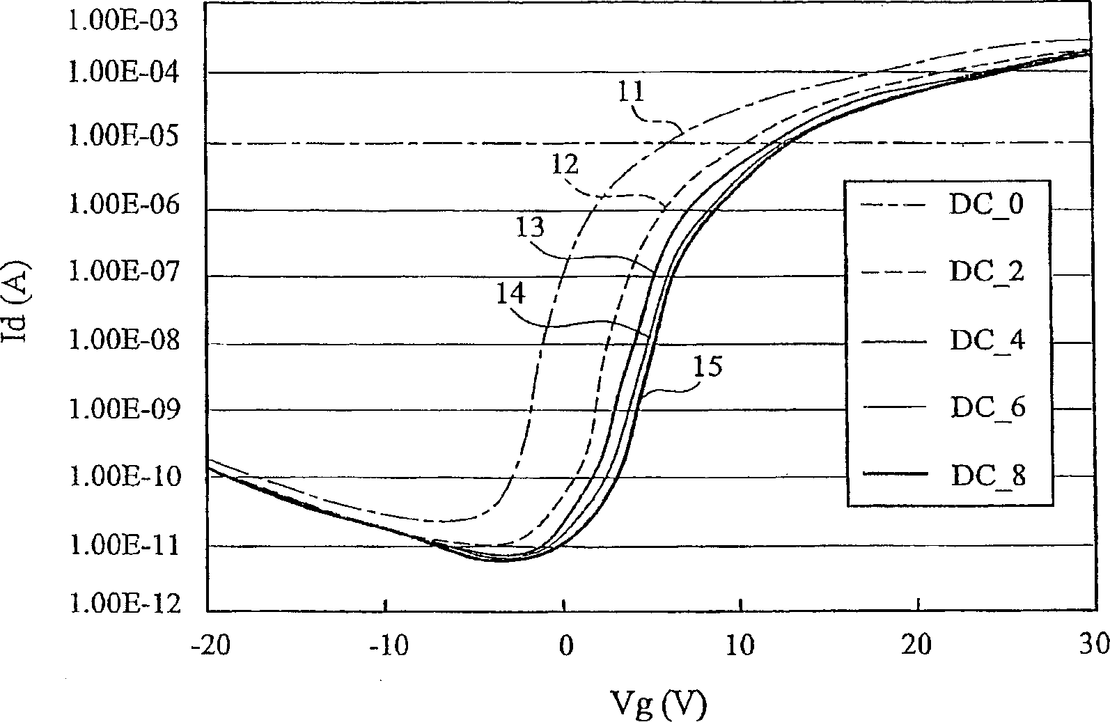
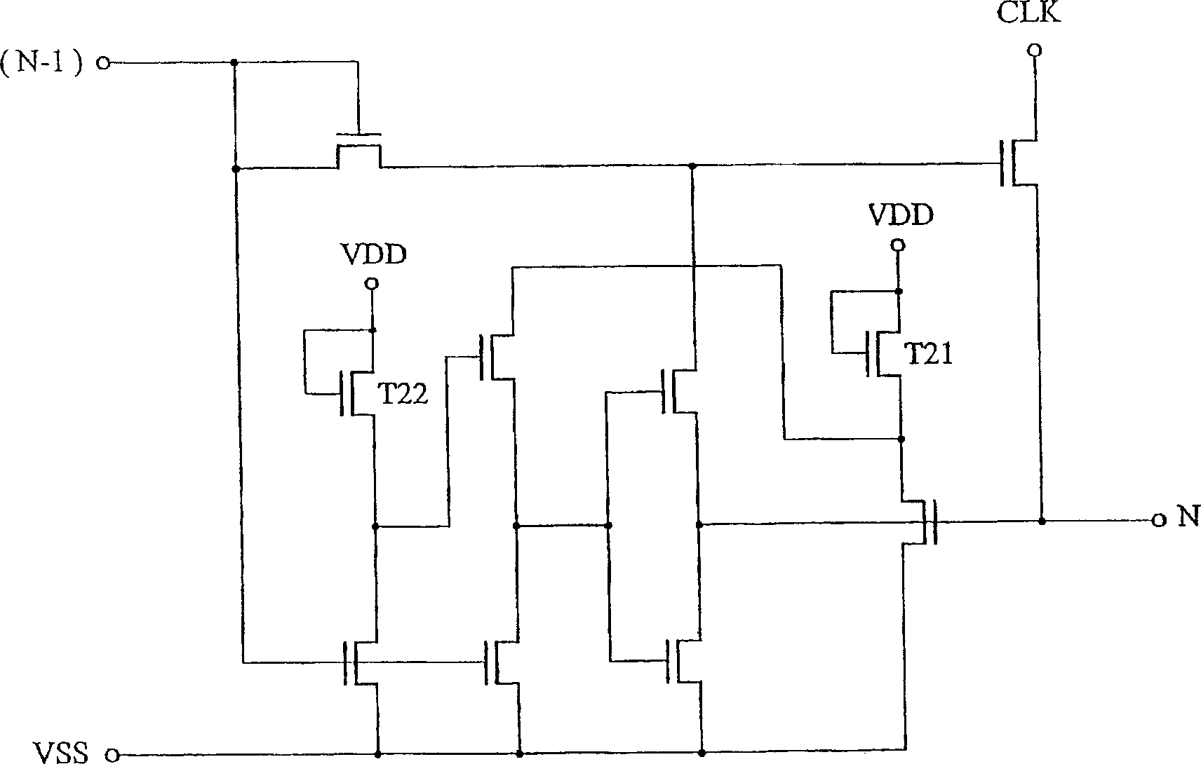
[0027] Figure 4 is a schematic diagram of a shift register according to a first embodiment of the present invention picture . In the first embodiment, the first pull-down module 41 and the second pull-down module 42 are used to alternately couple the output signal N of the shift register to the low voltage source VSS to maintain the output signal N in an off state. The gate of the transistor T41 and its first source / drain are coupled to the output signal (N−1) of the preceding shift register and the first pull-down module 41 . The second source / drain of the transistor T41 is coupled to the gate of the transistor T42. The first source / drain of the transistor T42 is coupled to a first clock signal CLK, and the second source / drain of the transistor T42 is coupled to the first pull-down module 41 , the second pull-down module 42 and the output signal N of the shift register. The first pull-down module 41 and the second pull-down module 42 are respectively coupled to the first c...


PUM


Abstract

The invention relates to a shift register circuit, which possesses a plurality of series-connected stage shift register including a first transistor with the grid and the first resource/leakage connecting with output signal of the front stage register. The second transistor with the grid is connected with the second resource/leakage electrode of the first transistor; the first resource/leakage electrode is connected with a first clock signal, the second resource/leakage electrode is connected with the output end of the second resource/leakage electrode. The first lower module is coupled with the output end and the first clock signal; when the output signal and the first clock signal of the front stage shift register are connected with the low voltage level, it coupled with the first voltage level. The second lower module is coupled with the output end and the second clock signal; when the output signal and the second clock signal of the front stage shift register are connected with the low voltage level, it coupled with the first voltage level.

Description

technical field [0001] The invention relates to a driving circuit of a liquid crystal display, in particular to a driving circuit of a shift register in the driving circuit of a liquid crystal display. Background technique [0002] Designing the driving circuit on the glass substrate of the liquid crystal display panel has become a main technology of the future liquid crystal display, and its biggest advantage lies in saving the cost of the driving IC. For thin film transistor displays, the process of amorphous silicon has become the mainstream at present, but for amorphous silicon thin film transistors, its instability, such as the voltage shift of the threshold voltage, has become the biggest problem in circuit design. Please refer to figure 1 , figure 1 It is a schematic representation of the voltage and current of a 300um process thin film transistor at 80°C and different operating times picture . Curves 11, 12, 13, 14 and 15 are the voltage and current curves of th...

Claims


Application Information

Patent Timeline
IPC IPC(8): G11C19/28G09G3/36
Inventor 魏俊卿吴仰恩林威呈
Owner AU OPTRONICS CORP
Why Eureka
Try Eureka