Defects detection method and apparatus for optical components

A technology for detecting optical components and defects, which is applied in the direction of optical testing defects/defects, testing of machines/structural components, measuring devices, etc. Problems such as the state of light emission, to achieve the effect of improving productivity

Inactive Publication Date: 2006-05-10
SHARP KK
View PDF2 Cites 5 Cited by
  • Summary
  • Abstract
  • Description
  • Claims
  • Application Information

AI Technical Summary

Problems solved by technology

Therefore, light is emitted from the protective sheet even when there is no defect, so it is not possible to clearly distinguish the state of light emission when there is a defect and when there is no defect, and it is not possible to detect defects of the multilayer polarizing element...

Method used


Image

  • Defects detection method and apparatus for optical components
  • Defects detection method and apparatus for optical components
  • Defects detection method and apparatus for optical components

Examples


Embodiment Construction

[0106] Hereinafter, preferred embodiments of the present invention will be described in detail with reference to the accompanying drawings.

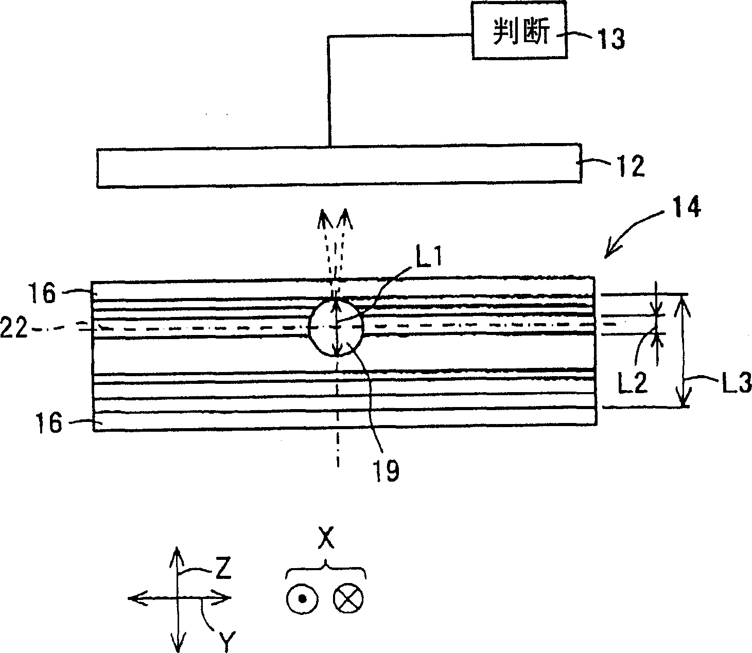
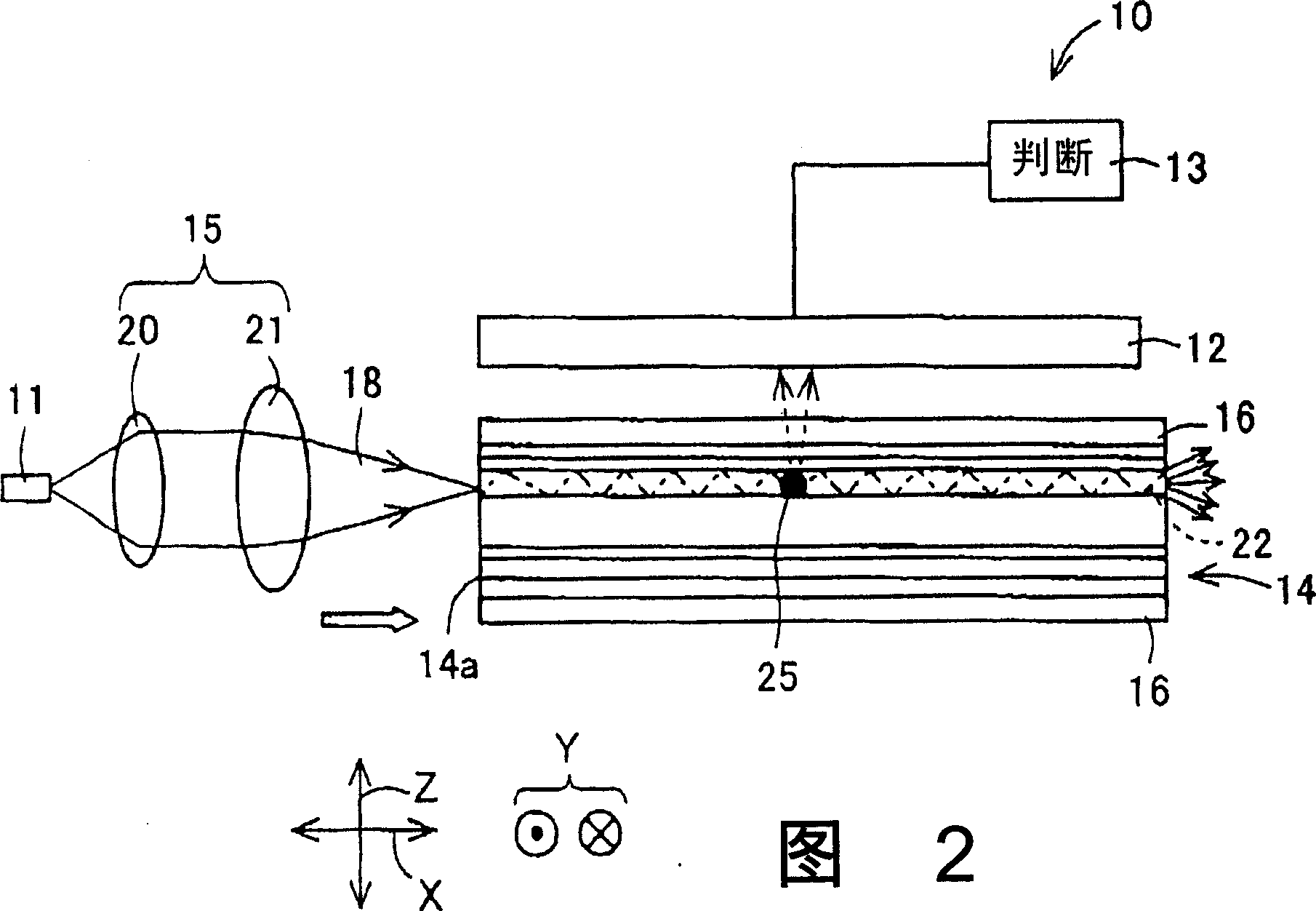
[0107] figure 1 It is a front view showing a part of an optical component defect inspection device 10 according to an embodiment of the present invention. FIG. 2 is a side view showing the optical component defect inspection device 10 . The composition of the optical component defect inspection device (hereinafter sometimes simply referred to as "defect inspection device") 10 includes a laser light source 11 , a light detection unit 12 , a judgment unit 13 and an incident unit 15 . The defect inspection device 10 detects a defect 25 in the optical component 14 formed by laminating a plurality of transmissive layers.

[0108] The optical member 14 is made of various materials, and in this embodiment, a plurality of sheet-like materials with different thickness dimensions are stacked in the thickness direction to form a multilayer struc...


PUM


Abstract

The invention discloses a defect detection method and a defect detection device of an optical component, wherein the judging part (13) makes the dimension L1 of the lamination direction of the incident area (19) larger than the thickness L2 of the light guide layer (22) of the optical component (14) way of incidence. The detection light (18) can enter the light guide layer (22) even if the positioning accuracy of the incident position of the detection light (18) is low. The judging unit (13) makes the detection light (18) incident so as to be smaller than the dimension L3 of the lamination direction of the optical member (14). The detection light (18) can be prevented from being scattered by scattering factors such as dust and scratches on both end faces of the optical member (14) in the stacking direction Z. Therefore, the defect (25) of the optical component (14) can be detected with high precision by detecting the light emitted from the optical component (14).

Description

field of invention [0001] The present invention relates to an optical component defect inspection method and a defect inspection device for detecting defects in an optical component formed by laminating a plurality of transmissive layers. Background technique [0002] Figure 24 It is a perspective view showing a defect inspection device 1 for a transparent substrate according to the first prior art. Japanese Patent Publication No. H11-190700 describes the first prior art. Laser 2 emits laser light 2 a toward mirror 3 . Mirror 3 directs laser light 2 a from laser 2 to converging lens 4 . Converging lens 4 directs the laser light from mirror 3 to transparent substrate 5 . The light incident on the transparent substrate is repeatedly reflected on both end surfaces in the thickness direction of the transparent substrate 5 . When the transparent substrate 5 has a defect, the defect causes light to scatter, and the scattered light is emitted to the outside of the transparent ...

Claims


Application Information

Patent Timeline
IPC IPC(8): G01M11/00G01N21/88
Inventor 三宅知之南功治平野兼史中田泰男仓田幸夫
Owner SHARP KK
Why Eureka
Try Eureka