Semiconductor memory

一种存储器、半导体的技术,应用在静态存储器、数字存储器信息、信息存储等方向,能够解决器件面积增大等问题

Inactive Publication Date: 2006-05-10
SOCIONEXT INC
View PDF1 Cites 3 Cited by
  • Summary
  • Abstract
  • Description
  • Claims
  • Application Information

AI Technical Summary

Problems solved by technology

This leads to an increase in the area of ​​the device

Method used


Image

  • Semiconductor memory
  • Semiconductor memory
  • Semiconductor memory

Examples


Embodiment Construction

[0039] Embodiments of the present invention will be described in detail below with reference to the accompanying drawings.

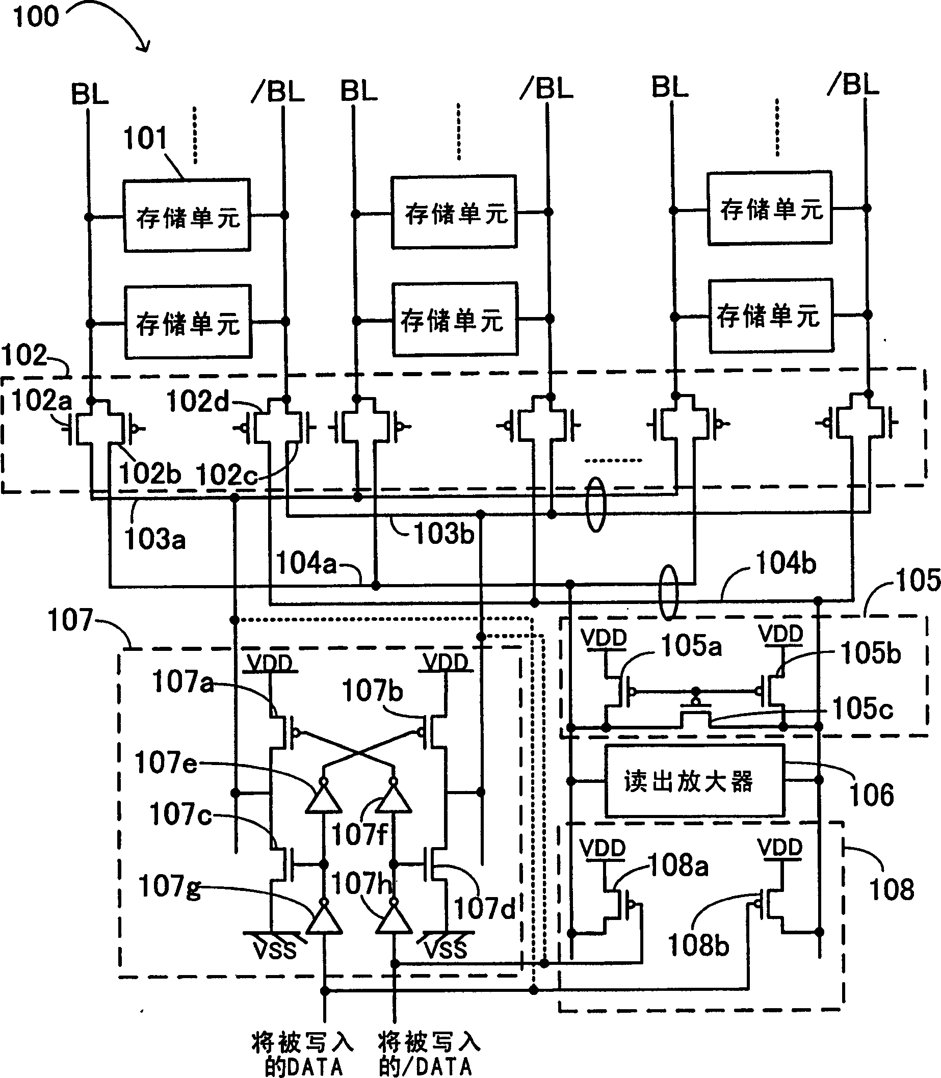
[0040] figure 1 is a circuit diagram of the semiconductor memory according to the first embodiment of the present invention.

[0041] The semiconductor memory 100 according to the first embodiment of the present invention includes a plurality of memory cells 101, a column selection circuit 102, write data buses 103a and 103b, read data buses 104a and 104b, a precharge circuit 105, a sense amplifier 106, a write An input amplifier 107 and a voltage boosting circuit section 108, wherein the plurality of memory cells 101 are arranged in the direction of rows and columns like a matrix, and are connected between complementary bit lines BL and / BL. exist figure 1 , the word lines WL connected to the plurality of memory cells 101 are not shown (see Figure 5 ).

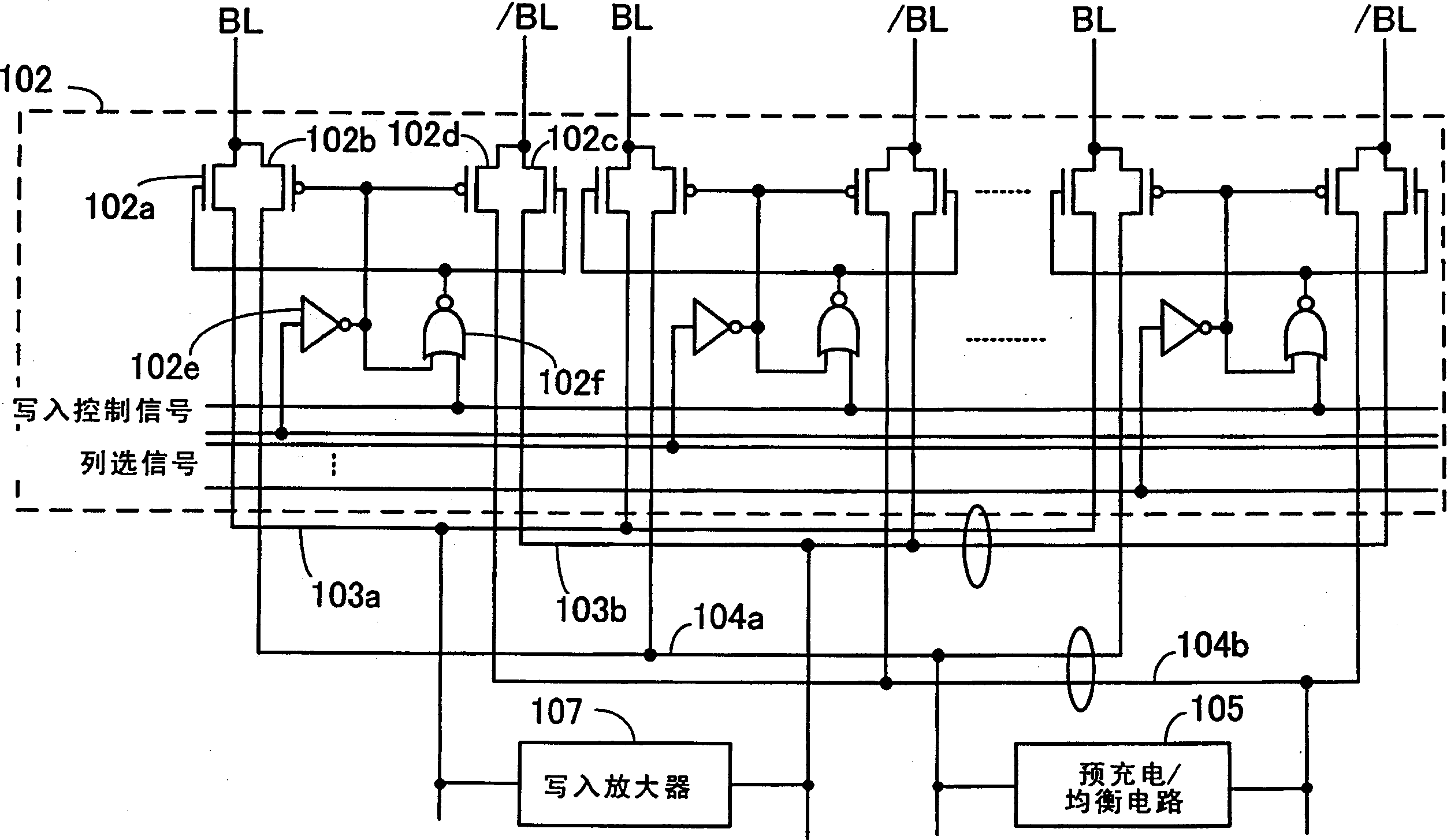
[0042] The column selection circuit 102 selects the bit lines BL and / BL in response to the co...


PUM


Abstract

The present invention discloses a semiconductor memory in which a drop in potential of a bit line due to coupling capacitance at the time of data writing can be restored in a space-saving manner without increasing load at the time of reading. The selection circuit selects the complementary bit line in response to the selection signal, and connects the selected complementary bit line to the write data bus or the read data bus. When writing data, the voltage boosting circuit section selects a read data bus to which one of the bit lines of the complementary bit line pair is connected based on the data to be written, and raises the potential of the selected read data bus, wherein The selected bit line is located opposite to the lowered bit line. In this way, the potential level that has been lowered due to the influence of the coupling capacitance between the bit lines can be restored.

Description

technical field [0001] The present invention relates to a semiconductor memory, and more particularly, the present invention relates to a semiconductor memory having a plurality of memory cells arranged in a row and column direction like a matrix and connected between complementary bit lines between. Background technique [0002] Figure 5 A circuit diagram showing an example of memory cells included in a static random access memory (SRAM). [0003] A memory cell 700 in an SRAM includes n-channel metal oxide semiconductor (MOS) field effect transistors (NMOS) 701 and 702 and inverters 703 and 704 between complementary bit lines BL and / BL. One input-output terminal of the NMOS 701 is connected to the bit line BL, and one input-output terminal of the NMOS 702 is connected to the bit line / BL. The other input-output terminal of the NMOS 701 is connected to the input terminal of the inverter 703 , and the other input-output terminal of the NMOS 702 is connected to the output ...

Claims


Application Information

Patent Timeline
Patent Type & Authority Applications(China)
IPC IPC(8): G11C11/419G11C7/00
CPCG11C7/1048G11C11/413G11C2207/002G11C2207/005E06B3/4609E06B7/00
Inventor 儿玉刚
Owner SOCIONEXT INC
Why Eureka
Try Eureka