Migration-proof light-emitting semiconductor device and method of fabrication

A technology for light-emitting components and semiconductors, which is applied to semiconductor devices, electrical components, and electric solid-state devices, etc., can solve the problem that light-emitting semiconductor regions do not effectively utilize light extraction, and achieve the effects of preventing short circuits and suppressing leakage currents.

Inactive Publication Date: 2006-05-10
SANKEN ELECTRIC CO LTD
View PDF1 Cites 16 Cited by
  • Summary
  • Abstract
  • Description
  • Claims
  • Application Information

AI Technical Summary

Problems solved by technology

[0010] In addition, in the traditional semiconductor light-emitting element, there is a problem that the side surface of the light-emitting semiconductor region does not effectively utilize the light extraction.

Method used


Image

  • Migration-proof light-emitting semiconductor device and method of fabrication
  • Migration-proof light-emitting semiconductor device and method of fabrication
  • Migration-proof light-emitting semiconductor device and method of fabrication

Examples


Embodiment 1

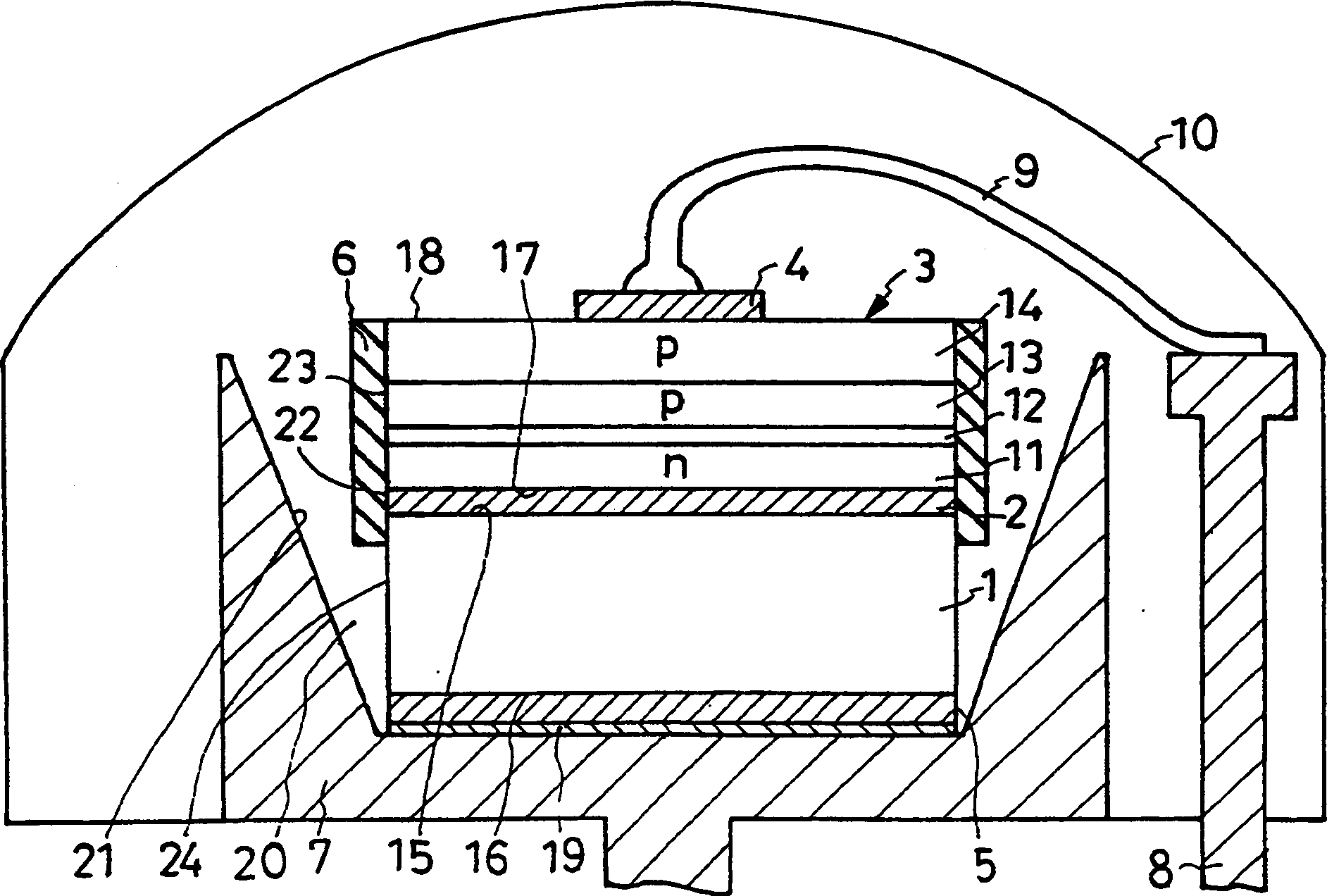
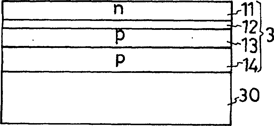
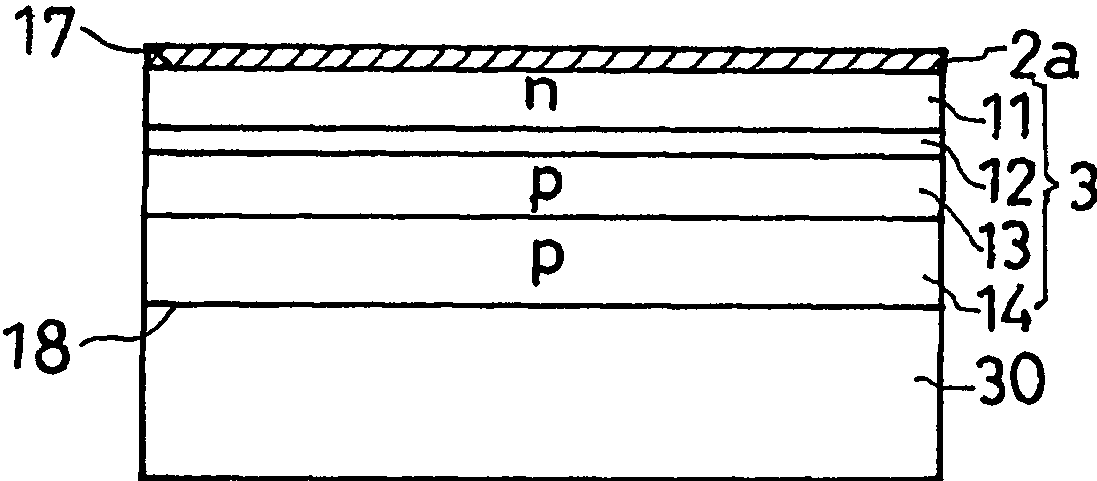
[0042] figure 1The light-emitting diode shown as the semiconductor light-emitting element of Embodiment 1 of the present invention is generally composed of the following parts: a conductive support substrate 1, a light reflection layer 2 made of a conductor layer, and a semiconductor region 3 with a light-emitting function. , the first electrode 4 , the second electrode 5 , the protective layer 6 , the mount 7 , the lead member 8 , the wire 9 and the resin enclosure 10 . In order to form a light-emitting diode with a double heterojunction structure, the semiconductor region 3 includes an n-type semiconductor layer 11 generally called an n-type cladding layer, an active layer 12, a p-type semiconductor layer 13 generally called a p-type cladding layer, and a p-type auxiliary layer. semiconductor layer 14 . The semiconductor region 3 will be described in detail later.

[0043] The support substrate 1 is composed of a conductive silicon semiconductor including one main surface ...

Embodiment 2

[0109] Below, explain Figure 8 The semiconductor light-emitting element of Example 2 is shown. but, Figure 8 and represent Examples 3 to 8 described later Figure 9 to Figure 14 basically with figure 1 The same symbols are used for the same parts, and descriptions thereof are omitted. and also, Figure 8 ~ Figure 14 The semiconductor light-emitting element shown is also provided with figure 1 The mounting seat 24, the lead terminal 8, the wire 9 and the same part of the enclosure 10, but in order to simplify Figure 8 ~ Figure 14 The illustration is omitted.

[0110] Figure 8 In the semiconductor light-emitting element of Example 2 except the deformed protective layer 6a and figure 1 same. Figure 8 The protective layer 6a is formed by making the exposed surface of the light reflection layer 2 and the exposed side surface of the semiconductor region 3 high-resistance, that is, insulated. This insulating protection layer 6 a can be formed by implanting ions into th...

Embodiment 3

[0113] Figure 9 The semiconductor light-emitting element of Example 3 shown is in addition to the deformed protective layer 6b and the current blocking layer 31 and figure 1 The same constitutes.

[0114] Figure 9 The protective layer 6b consists of the first protective layer 6b covering the side 22 of the light reflection layer 2 1 and cover the first protective layer 6b 1 The second protective layer 6b on 2 constitute. First protective layer 6b 1 and Figure 8 The protective layer 6a is also formed by ion implantation. Second protective layer 6b 2 and figure 1 The protective layer 6 is also formed by coating an insulating inorganic substance, except for covering the first protective layer 6b 1 In addition, the side surface 23 of the semiconductor region 3 , the other main surface 18 and part of the side surface of the substrate 1 are also covered. Figure 9 The side surface 22 of the light reflection layer 2 is covered by the first and second protective layers 6...


PUM


Abstract

The semiconductor light-emitting element of the invention comprises a conductive support substrate (1), a semiconductor region (3) and a light-reflecting layer (2) with light-emitting functions. The semiconductor region (3) includes an n-type semiconductor layer (6), an active layer (7), a p-type semiconductor layer (8) and a p-type auxiliary semiconductor layer (9). The light reflection layer (2) is made of Ag or Ag alloy, and is arranged between the semiconductor region (3) and the supporting substrate (1). The light reflection layer (2) is formed by bonding the first adhesive layer made of Ag or Ag alloy formed on one main surface of the semiconductor region (3) and the first adhesive layer made of Ag or Ag alloy formed on one main surface of the supporting substrate (1). Alloy composition of the second adhesive layer to form. Either one or both of the side (22) of the light reflection layer (2) and the side (23) of the semiconductor region (3) are covered with a protective layer (6) for inhibiting migration.

Description

technical field [0001] The present invention relates to a semiconductor light emitting element used for a display, a lamp, and the like, and a method for manufacturing the same. Background technique [0002] The semiconductor region with light-emitting function of the semiconductor light-emitting element includes: an n-type semiconductor layer generally called an n-type cladding layer, an active layer, and a p-type semiconductor layer generally called a p-type cladding layer. In a general semiconductor light emitting element, one of the paired main surfaces of the semiconductor region having a light emitting function serves as a light extraction surface. However, light is emitted from the active layer not only to one main surface side of the semiconductor region but also to the other main surface side. Therefore, in order to improve the light extraction efficiency of the semiconductor light emitting element, it is important to reflect the light emitted from the active layer...

Claims


Application Information

Patent Timeline
Patent Type & Authority Applications(China)
IPC IPC(8): H01L33/06H01L33/10H01L33/32H01L33/34H01L33/56H01L33/62
CPCH01L33/44H01L24/32H01L2224/32245H01L2224/48247H01L2224/48465H01L2224/73265H01L2924/0133H01L2924/12041H01L2924/01012H01L2924/01029H01L2224/48091H01L33/0093H01L2924/00H01L2924/01031H01L2924/01032H01L2924/01079H01L2924/3512H01L2924/00014
Inventor 青柳秀和加藤隆志松尾哲二
Owner SANKEN ELECTRIC CO LTD
Why Eureka
Try Eureka