Film stress test method and test structure

A film stress, testing structure technology, applied in measurement devices, surface/boundary effects, instruments, etc., can solve the problems of increasing testing complexity, equipment complexity, restricting application, etc. The effect of systematic error, detection accuracy and sensitivity improvement

Inactive Publication Date: 2006-06-28
PEKING UNIV
View PDF0 Cites 20 Cited by
  • Summary
  • Abstract
  • Description
  • Claims
  • Application Information

AI Technical Summary

Problems solved by technology

The problem is equally severe with more complex modeled plane displacement test structures
[0005] 2) Incorrect geometric dimension input will also affect the measurement results: including process errors such as the shape and dimension of the microstructure, the angle between the support part and the substrate, over-etching, etc., which seriously affect the measurement accuracy
[0006] 3) The solution of the stress of the film is often established under the condition that the Young's modulus and Poisson's ratio of the film are known, and these mechanical parameters of the material are also closely related to the process conditions, which need to be accurately extracted through certain testing methods, or through complex Arrays or loads are decoupled, increasing the complexity of testing
[0008] With the rise of Nano-Electro-Mechanical System (Nano-Electro-Mechanical System) research, the detection of mechanical properties of structural materials at the nanoscale has also become a research hotspot. At present, there are few reports on the test of nanoscale film stress. Some foreign scholars use SEM / TEM / AFM and other equipment combined with a plane displacement test structure for measurement, but the equipment is complex and needs to be operated in a special environment such as vacuum, which seriously restricts its application

Method used


Image

  • Film stress test method and test structure
  • Film stress test method and test structure
  • Film stress test method and test structure

Examples


Embodiment Construction

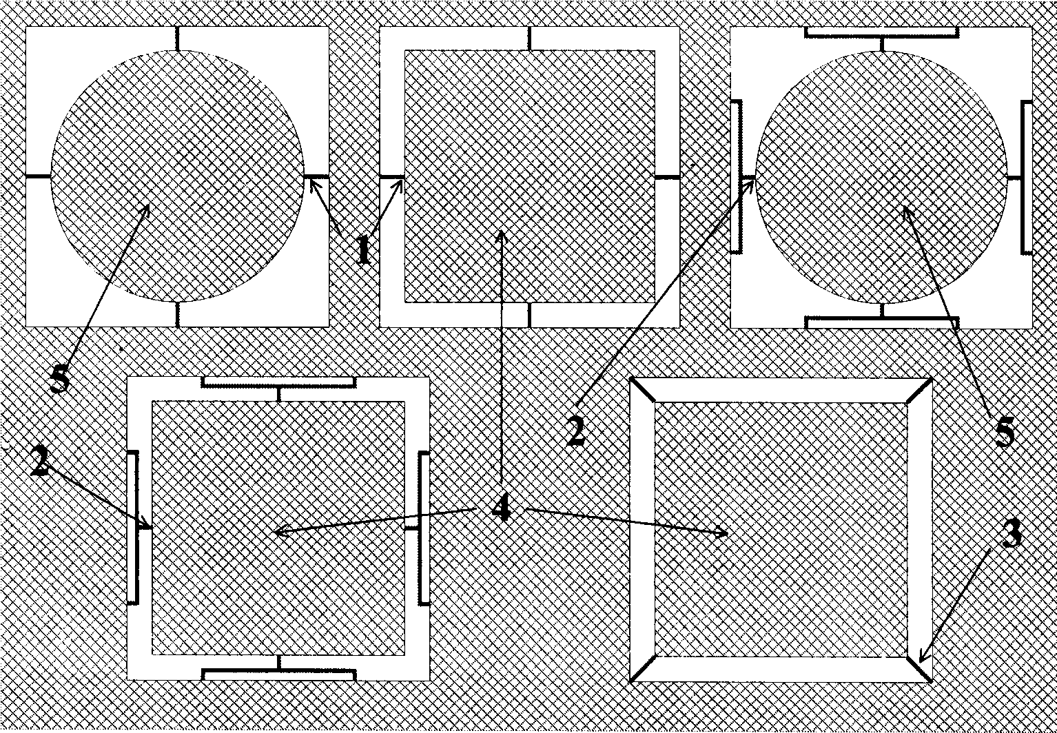
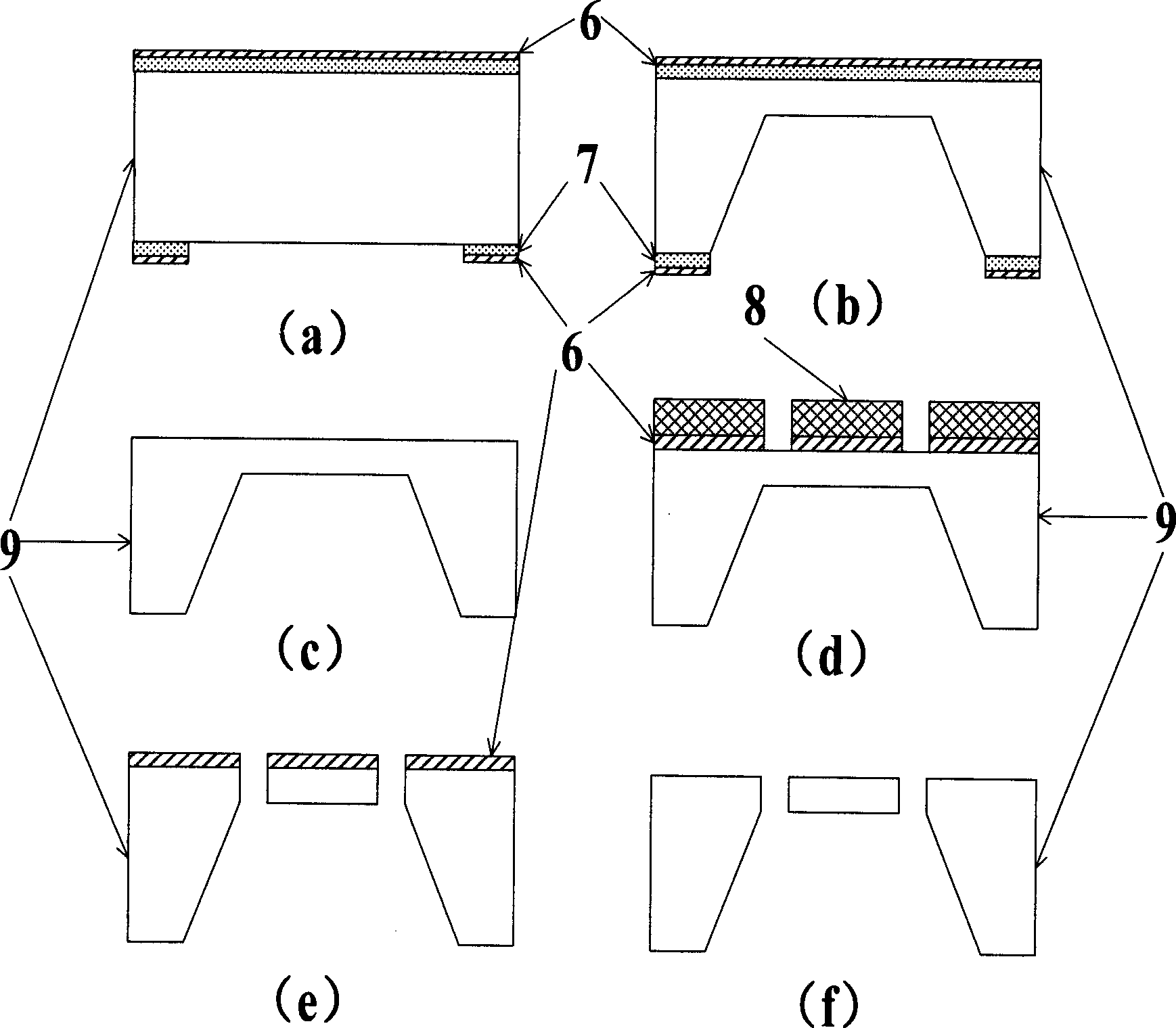
[0035] The test structure is shown as figure 1 , structures 1, 2, and 3 are support structures, respectively, and test structures 4 and 5 are circular and square suspended structures. The size of the suspended structure is 1mm×1mm. Since the test structure has a fixed support, the constraint conditions are the same during the test of the curvature radius before and after the deposition of the film, so that the influence of gravity can be eliminated. Secondly, in the range of 1×1mm, the thickness of the silicon wafer and the non-uniformity of the deposited film are greatly reduced, reducing the error. Since the silicon film is thinned to 15 μm, which is only 1 / 30 of the thickness of the wafer substrate, according to the formula (1), its resolution is greatly improved.

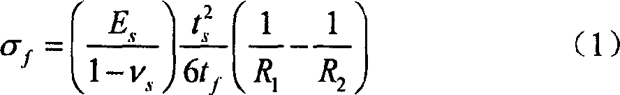
[0036] The substrate bending method obtains the stress of the film by measuring the radius of curvature of the substrate before and after film deposition, which is expressed by formula (1) as follows:

[0037]...


PUM

PropertyMeasurementUnit
thicknessaaaaaaaaaa
thicknessaaaaaaaaaa
thicknessaaaaaaaaaa

Abstract

A method for testing film stress includes concentrating test range on partial substrate, decreasing thickness of this partial substrate and designing fixed support structure, obtaining film stress deposited on substrate by measuring the bending curvity of this partial substrate before and after film is deposited.

Description

technical field [0001] The invention belongs to the technical field of micro-electro-mechanical system (MEMS) testing, and in particular relates to a high-sensitivity thin-film stress testing method and testing structure. Background technique [0002] Films prepared by MEMS surface micromachining often have non-negligible residual internal stress. For typical microstructures using surface micromachining, such as cantilever beams, microbridges, and microdiaphragms, the internal stress of the film will directly affect important static and dynamic design parameters such as the stiffness and resonance frequency of the device, and directly affect the performance of the designed device, even cause device failure. Accurate measurement of film stress provides the necessary basis for process design and device simulation. [0003] In recent years, people have developed many plane stress test structures based on surface micromachining technology, and the stress can be determined acco...

Claims


Application Information

Patent Timeline
Patent Type & Authority Applications(China)
IPC IPC(8): G01N13/00
Inventor 陈兢王莎莎
Owner PEKING UNIV
Why Eureka
Try Eureka