Preparation method of polycrystalline vanadium dioxide film with room temperature resistance temperature coefficient higher than 10%K

A technology of temperature coefficient of resistance and vanadium dioxide is applied in the field of polycrystalline vanadium dioxide thin film preparation, which can solve the problems of affecting the detection rate of the device, cannot be used, high TCR, etc., and achieves low grain boundary density, increased activation energy, and improved TCR. Effect

Active Publication Date: 2006-07-12
溧阳常大技术转移中心有限公司
View PDF2 Cites 12 Cited by
  • Summary
  • Abstract
  • Description
  • Claims
  • Application Information

AI Technical Summary

Problems solved by technology

Since the film prepared by the sol-gel method cannot meet the last three requirements, even if a higher TCR can be obtained, it can only be used as a mechanism study and cannot be actually used in device preparation.
Thin films prepared by other methods are difficult to obtain a high TCR. Although they can be used as sensitive films for infrared detection and imaging devices, they affect the detection rate of the devices.

Method used


Image

  • Preparation method of polycrystalline vanadium dioxide film with room temperature resistance temperature coefficient higher than 10%K
  • Preparation method of polycrystalline vanadium dioxide film with room temperature resistance temperature coefficient higher than 10%K
  • Preparation method of polycrystalline vanadium dioxide film with room temperature resistance temperature coefficient higher than 10%K

Examples


Embodiment Construction

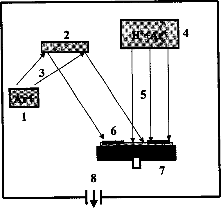
[0025] The preparation process of the embodiment of the present invention is as follows:

[0026] (1) Preparation of sputtering target

[0027] High-purity V with a purity of 99.99% 2 o 5 Powder and high purity Sb with a purity of 99.99% 2 o 3 、 Ta 2 o 5 、WO 3 、MoO 3 , MnO, Nb 2 o 5 The powder is uniformly mixed and ball milled at 100atm%: 1-15atm%. In order to prevent the introduction of impurities, agate balls and agate jars are used for ball milling, and the speed of ball milling is controlled at 40-60 revolutions per minute. at 100Kg / cm 2 The initial pressure molding, and then 2000Kg / cm 2 , 20 minutes of isostatic pressing to obtain a solid sputtering target. Finally, heat treatment in an air atmosphere in a box furnace. The heating rate is about 5°C / min when the temperature is 300°C-600°C, and it is kept at 600°C for one hour. After cooling down to room temperature naturally, take it out for use.

[0028] (2) Ion beam enhanced deposition

[0029] The sputte...


PUM

PropertyMeasurementUnit
densityaaaaaaaaaa

Abstract

The invention relates to a functional thin film material preparing technology, which adopts improved ion beam amplify deposited method to make the film and combines the subsequent crystallization and annealing to achieve the impurity element even immersing and the effective place-replacing to vanadium so that the phase starting temperature of the thin film reduces to 12-16 deg. It adjusts the argon / hydrogen ratio film craft and crystallizing heat treatment condition so that when the polycrystalline VO2 thin film transfers to the mental phase from the semiconductor phase, the change of the resistance ratio over 2 magnitude orders.

Description

technical field [0001] The invention relates to a preparation technology of a functional thin film material, in particular to a preparation method of a polycrystalline vanadium dioxide thin film with a temperature coefficient of resistance (TCR) at room temperature higher than 10% / K. Background technique [0002] Vanadium oxide thin film is an important sensitive film for preparing uncooled focal plane infrared imaging array (UFPA) and infrared detector. Its preparation methods mainly include magnetron sputtering deposition, ion beam sputtering, laser pulse deposition mentioned in Chinese patent 200410060770.1 "Preparation method of vanadium oxide thin film with adjustable phase transition temperature", Chinese patent 03115643.6 "vanadium oxide thin film material Preparation method " mentioned sol-gel method etc. Although vanadium oxide thin films can be prepared by various methods, the properties, cost, and manufacturability of the resulting thin films vary. At present, t...

Claims


Application Information

Patent Timeline
Patent Type & Authority Applications(China)
IPC IPC(8): C23C14/34C23C14/08
Inventor 李金华袁宁一
Owner 溧阳常大技术转移中心有限公司
Why Eureka
Try Eureka