Method of laser processing a wafer

A laser processing method and laser processing technology, used in laser welding equipment, metal processing equipment, manufacturing tools, etc., can solve problems such as device damage and achieve the effect of increasing pulse energy

Inactive Publication Date: 2006-07-19
DISCO CORP
View PDF1 Cites 12 Cited by
  • Summary
  • Abstract
  • Description
  • Claims
  • Application Information

AI Technical Summary

Problems solved by technology

However, if the wafer is irradiated with a high-power laser beam, the film layer may be peeled off by about 100 to 200 μm on one side due to the impact of the laser beam irradiation, and there is a problem that the device is damaged.

Method used


Image

  • Method of laser processing a wafer
  • Method of laser processing a wafer
  • Method of laser processing a wafer

Examples


Embodiment Construction

[0023] Hereinafter, the wafer dividing method according to the present invention will be described in more detail with reference to the drawings.

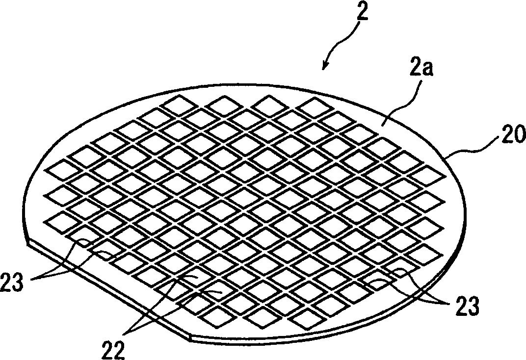
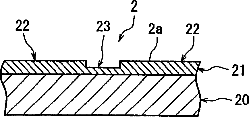
[0024] figure 1 A perspective view showing an optical device wafer divided into individual chips by the wafer dividing method of the present invention, figure 2 express figure 1 An enlarged cross-sectional view of the main part of the optical device wafer shown. figure 1 and figure 2 In the shown optical device wafer 2, a plurality of devices 22 are formed in a matrix form on the surface of a substrate 20 such as quartz or borosilicate glass, by laminating a film layer 21 having a wavelength selection filter function. For example, the above-mentioned film passes only light of a specific wavelength or a specific range of wavelengths, and reflects light of other wavelengths. Furthermore, each device 22 is divided by dicing lines 23 formed in a lattice. Also, in the illustrated embodiment, the film forming the film layer 21 is ...


PUM

PropertyMeasurementUnit
particle diameteraaaaaaaaaa
energyaaaaaaaaaa

Abstract

A method of laser processing a wafer having a plurality of devices that are composed of a laminate layer laminated on the front surface of a substrate, along a plurality of streets for sectioning the devices, comprising a first groove forming step for applying a first laser beam having absorptivity for the wafer along the streets of the wafer at predetermined intervals to form two grooves for preventing the flaking of a layer, which divide the laminate layer; and a second groove forming step for applying a second laser beam having absorptivity for the wafer to the center between the two grooves for preventing the flaking of a layer, which have been formed along the streets of the wafer by the first groove forming step, along the streets of the wafer to form a dividing groove having a predetermined depth in the laminate layer and the substrate.

Description

technical field [0001] The present invention relates to a laser processing method of a wafer in which a plurality of devices are formed from film layers stacked on the surface of a substrate for performing laser processing along dicing streets formed on the surface of the wafer. Background technique [0002] As known to those skilled in the art, silicon oxide (SiO 2 ) and the like to select a film of a specific wavelength, and to form an optical device wafer in which a plurality of optical devices are formed in a matrix. The optical device wafer thus formed is divided into the plurality of optical devices by pre-segmentation lines called dicing lines, and each optical device is manufactured by dividing along the dicing lines. [0003] Separation of such an optical device wafer along a dicing line is generally performed by a cutting device called a dicing machine. This cutting device includes: a chuck table, which holds the workpiece, that is, an optical device wafer; a cut...

Claims


Application Information

Patent Timeline
Patent Type & Authority Applications(China)
IPC IPC(8): B23K26/36H01L21/301
CPCB23K26/367H01L21/78H01L21/3043B23K26/4075H01L21/67092B23K26/364B23K26/40B23K2103/50
Inventor 小林贤史
Owner DISCO CORP
Why Eureka
Try Eureka