

High-precision three-dimensional micro-assembling method and assembly parts based on MEMS
A micro-assembly and high-precision technology, applied in microstructure devices, processing microstructure devices, measurement devices, etc., can solve the problem of limited types of MEMS devices, incomplete optimization of device performance, and inability to realize hybrid integration of multiple MEMS devices, etc. problem, to achieve the effect of high-precision assembly
- Summary
- Abstract
- Description
- Claims
- Application Information
AI Technical Summary
Problems solved by technology
Method used
Image

Examples
Embodiment Construction
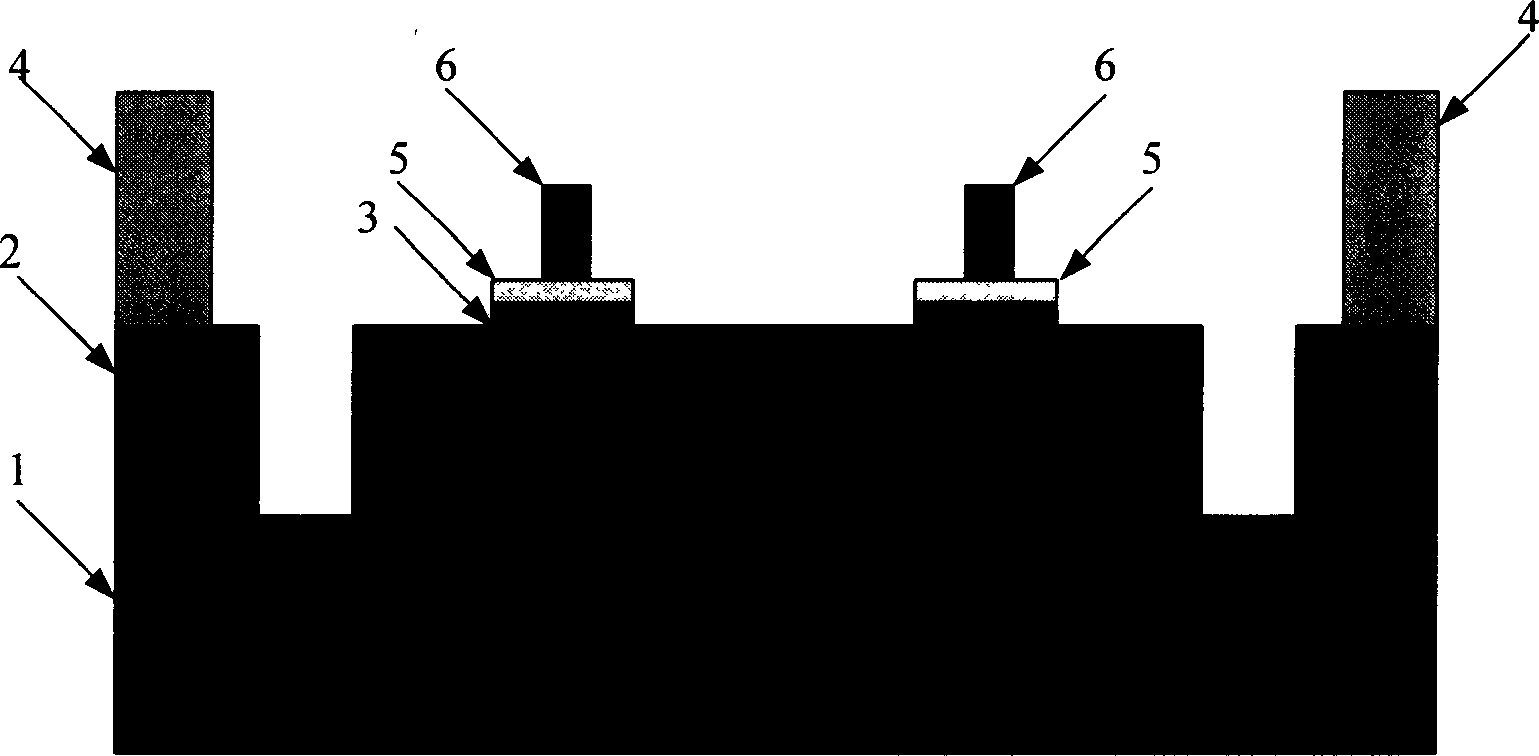
[0024] 1. Substrate preparation:
[0025] (1) growing an insulating layer such as silicon dioxide on the substrate;
[0026] (2) sputter metal adhesion layer and seed layer, and define metal interconnection;
[0027] (3) Define the position of the groove and plate the solder bump;
[0028] (4) Remove the seed layer and metal adhesion layer
[0029] (5) Use photosensitive polymer materials to make micro-fixtures, such as spin-coated SU8;
[0030] (6) Alignment grooves are formed by etching deep grooves in bulk silicon, see figure 1 .
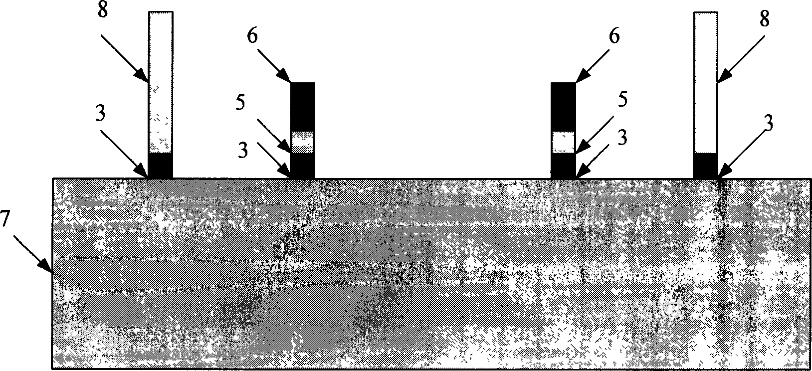
[0031] 2. Preparation of chips to be assembled:
[0032] (1) growing an insulating layer such as silicon dioxide on the substrate;
[0033] (2) sputter metal adhesion layer and seed layer, and define metal interconnection;
[0034] (3) Plating solder bumps;
[0035] (5) Plating alignment posts, such as metal Au;
[0036] (6) Remove the seed layer and metal adhesion layer, see figure 2 .
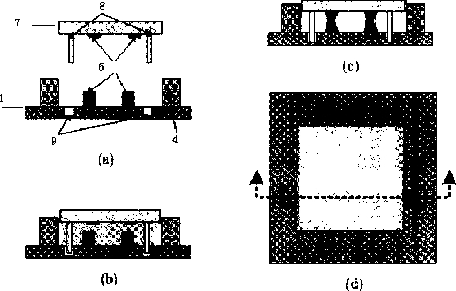
[0037] 3. Preliminary positioning using microg...
PUM
 Abstract
Description
Claims
Application Information