Batch manufacturing method for vertical structural semiconductive chip or device

A mass production, vertical structure technology, applied in the direction of semiconductor devices, electrical components, circuits, etc., can solve the problems affecting the quality of the light-emitting layer of the epitaxial layer, and achieve the effects of improving light extraction efficiency, reducing stress, and reducing contact resistance

Inactive Publication Date: 2006-08-02
ZHEJIANG INVENLUX TECH
View PDF2 Cites 11 Cited by
  • Summary
  • Abstract
  • Description
  • Claims
  • Application Information

AI Technical Summary

Problems solved by technology

However, the process of chemically stripping the growth substrate (such as etching) and the process of mechanically stripping the growth substrate (such as grinding) can affect the quality of the epitaxial layer (including the light-emitting layer)

Method used


Image

  • Batch manufacturing method for vertical structural semiconductive chip or device
  • Batch manufacturing method for vertical structural semiconductive chip or device
  • Batch manufacturing method for vertical structural semiconductive chip or device

Examples


Embodiment

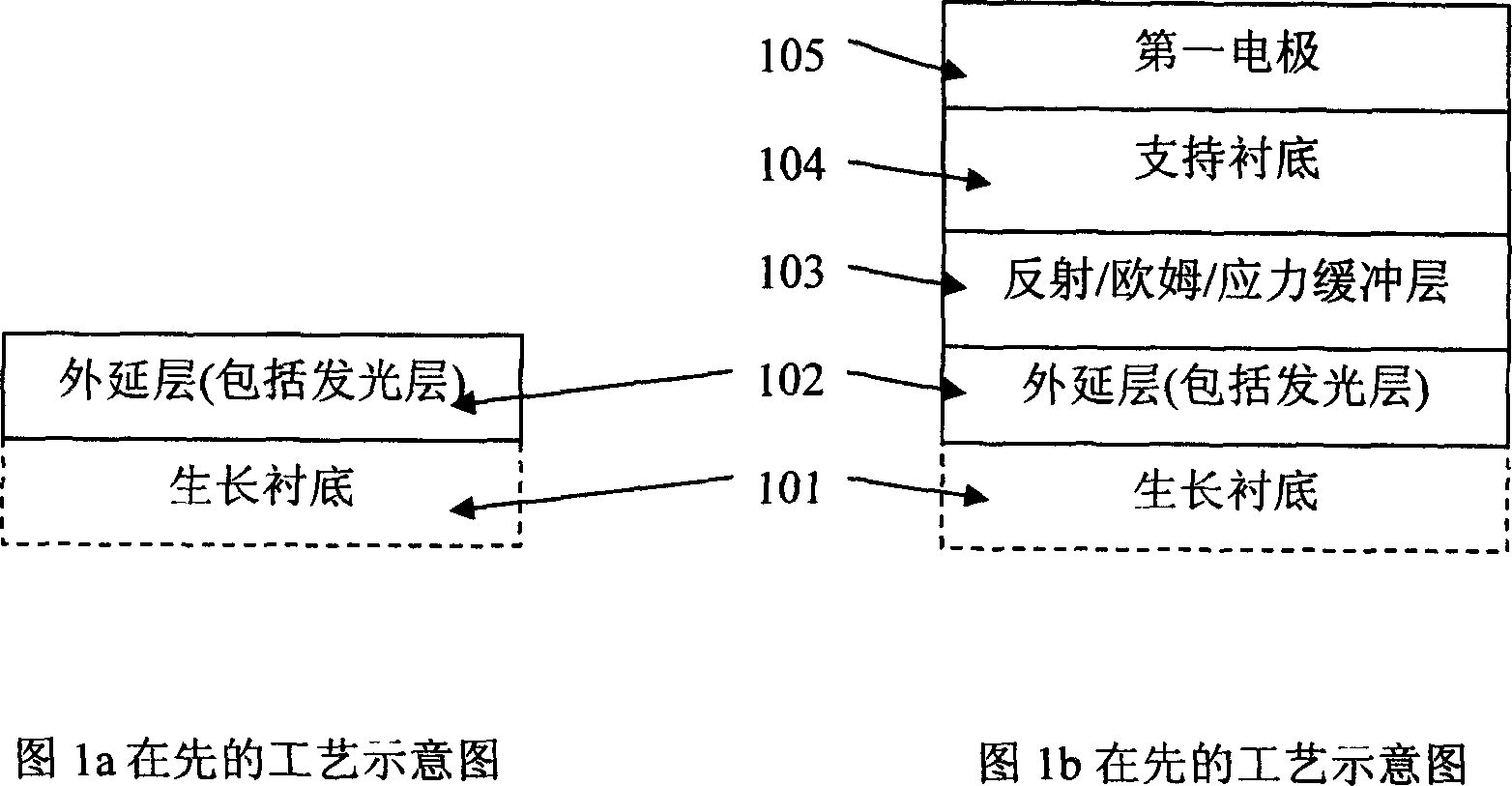
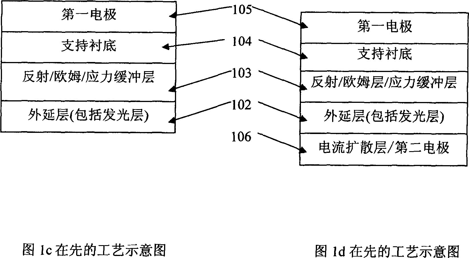
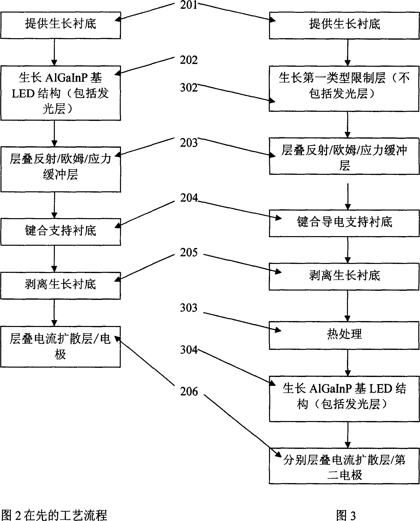
[0036] Process flow 304: a first specific implementation example: sequentially grow a light emitting layer and confine the second type on the first type confinement layer. A second specific implementation example: First, grow a first-type confinement layer on the exposed first-type confinement layer, and then grow a light-emitting layer and a second-type confinement layer sequentially on the new first-type confinement layer. The material of the light-emitting layer is selected from a group of materials including, but not limited to, gallium arsenide (GaAs), gallium phosphide (GaP), aluminum gallium arsenide (AlGaAs), aluminum gallium indium phosphide (AlGaInP) . The structure of the light-emitting layer includes, but not limited to, single quantum well, multiple quantum well, and bulk structure.

[0037] Process flow 206: stacking the current diffusion layer on the second type confinement layer, and stacking the second electrode on the current diffusion layer.

[0038] FIG. ...


PUM


Abstract

This invention discloses the high luminance semiconductor chip or device (concludes AlGaInP base LED) of vertical structure and low-cost high-output batch production method. The process of producing vertical structure AlGaInP base LED conclude: first, develop first style restricting layer on the developing substrate. Then, stack up reflecting/ ohm/ stress buffer layer on the first style restricting layer; bond electricity-conductive supporting substrate on the reflecting/ ohm/ stress buffer layer. The bonding side of electricity-conductive substrate and reflecting/ ohm/ stress buffer layer can has etched texture structure to reduce the stress of heat mismatching. First electrode stacks on the other side of electricity-conductive supporting substrate. When peeling off developing substrate, the first style restricting layer uncovers. There are developing illuminant layer, second style restricting layer, electric-current diffused layer and second electrode on the uncovered first style restricting layer.

Description

technical field [0001] The invention discloses a semiconductor chip or device with a vertical structure (including a high-brightness aluminum gallium indium phosphide (AlGaInP)-based semiconductor light-emitting diode (LED)) and a mass production method with low cost and high yield, belonging to the technical field of semiconductor optoelectronics. Background technique [0002] A lot of effort has been invested in vertical semiconductor chips or devices, and the production process of vertical aluminum gallium indium phosphide (AlGaInP)-based LEDs is very mature. [0003] US Patents 5,008,718, 5,376,580 and 5,502,316 disclose techniques for producing aluminum gallium indium phosphide (AlGaInP) based LEDs. The basic process is as follows, growing aluminum gallium indium phosphide (AlGaInP) epitaxial layer (including light-emitting layer) on a growth substrate (eg, gallium arsenide (GaAs)), laminating the support substrate, peeling off the growth substrate, Electrodes are stac...

Claims


Application Information

Patent Timeline
Patent Type & Authority Applications(China)
IPC IPC(8): H01L33/00
Inventor 彭晖罗威
Owner ZHEJIANG INVENLUX TECH
Why Eureka
Try Eureka