A low-emissivity film
A low-radiation, thin-film technology, applied in the direction of metal layered products, chemical instruments and methods, layered products, etc., can solve the problems of thin film manufacturing and parameter detection, complex preparation process, high production cost, etc., and achieve simplified film deposition Effects of process flow, increase in transmittance, and reduction in the number of layers
- Summary
- Abstract
- Description
- Claims
- Application Information
AI Technical Summary
Problems solved by technology
Method used
Image
Examples
Embodiment 1
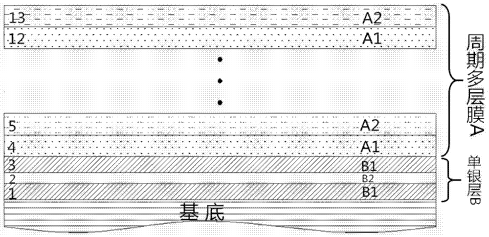
[0038] The thickness of the low-radiation film provided by Example 1 is 1410nm, including a single silver layer and a periodic multilayer film. Specifically, the thickness of the Ag film is 10nm, and the thickness of the TiO 2 The thickness of the protective layer is 25nm; in the periodic multilayer film, TiO 2 Film thickness is 106nm, SiO 2 The film thickness is 164nm; the central wavelength λ of the periodic multilayer film 0 950nm.
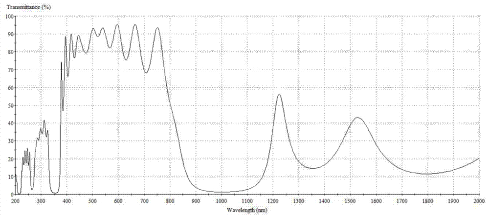
[0039] figure 2 Shown is the effect diagram of the transmittance of the low-emissivity film provided by Example 1 of the present invention. The transmittance of visible light is 70-96%, and the transmittance of most bands of visible light is above 85%, and the transmittance of ultraviolet bands is lower than 15%, the transmittance of the infrared band from 780nm to 1200nm is lower than 10%, and the transmittance of the infrared band from 1200nm to 3000nm reaches 25%.
Embodiment 2~7
[0041] The low-emissivity films provided in Examples 2-7 include a single silver layer and a periodic multilayer film, and the specific parameters are as shown in Table 1. The transmittances of the low-emissivity films provided in Examples 2-7 are shown in Table 2:
[0042] The film layer parameter list of table 1 embodiment 2~7
[0043]
[0044] Table 2 The transmittance table of each band of embodiment 2~7
[0045]
[0046] Analysis of the low-emissivity films provided in Examples 1 to 7 found that the thickness of the metal Ag film B2 was 9 nm to 12 nm, and the protective layer B1 TiO 2 The thickness is 10nm ~ 40nm and the center wavelength λ 0 The low-emissivity film in the range of 900nm to 1050nm, its transmittance fluctuates within a controllable range, the visible light transmittance ranges from 63% to 96%, and the transmittance of most bands of visible light is above 80%, and the average transmittance in the ultraviolet region 10%-18%, the transmittance in the...
PUM
| Property | Measurement | Unit |
|---|---|---|
| thickness | aaaaa | aaaaa |
| wavelength | aaaaa | aaaaa |
| thickness | aaaaa | aaaaa |
Abstract
Description
Claims
Application Information


