Unlock instant, AI-driven research and patent intelligence for your innovation.

Solid-state imaging apparatus

A solid-state imaging device and semiconductor technology, applied in the field of CMOS sensors, can solve the problems of increasing light shot noise, unsuitable pixel miniaturization, and reduction of saturated signals.

Inactive Publication Date: 2006-09-13
KK TOSHIBA
View PDF1 Cites 0 Cited by
  • Summary
  • Abstract
  • Description
  • Claims
  • Application Information

AI Technical Summary

Problems solved by technology

This leads to the problem of reducing the saturation signal of the pixel feature and increasing the light shot noise (ShotNoise)
[0004] In addition, in the case of CMOS sensors, it is difficult to use high-voltage drive and multiple power supplies such as CCD (Charge Coupled Device)
Therefore, there is a problem that the charge accumulated in the photodiode tends to be left over when the signal is read out, and this becomes the main cause of the afterimage.
[0005] However, in the case of this proposal, since the area of ​​the photoelectric conversion region becomes smaller due to miniaturization, it becomes difficult to form the gate electrode of the insulated gate transistor near the center of the potential recess. applicable structure

Method used


Image

  • Solid-state imaging apparatus
  • Solid-state imaging apparatus
  • Solid-state imaging apparatus

Examples


no. 1 approach

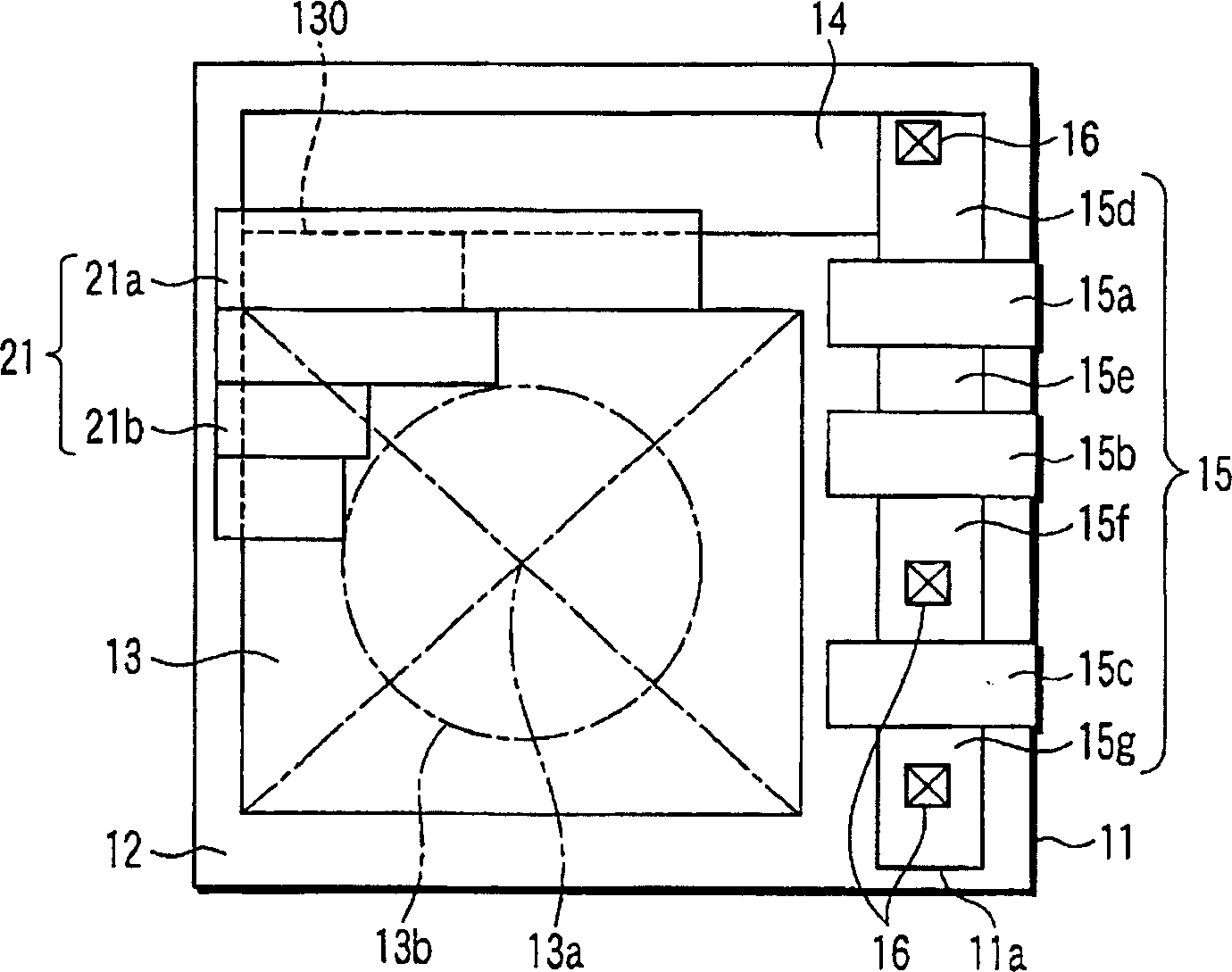
[0023] figure 1 The basic configuration of the CMOS sensor (solid-state imaging device) according to the first embodiment of the present invention is shown. Here, one pixel (unit element) constituting the pixel region of the CMOS sensor is shown as an example. However, wiring is omitted for convenience.

[0024] like figure 1 As shown, for example, an element isolation region 12 of an STI (Shallow Trench Isolation) structure is selectively formed in a surface region of a P-type semiconductor substrate (hereinafter referred to as a P-type substrate) 11 . In the active region defined by the element isolation region 12 of the P-type substrate 11, that is, in the surface region of the P-type substrate 11 other than the element isolation region 12, an embedded photodiode serving as a photoelectric conversion portion is formed. 13. A signal detection unit 14 and a signal scanning circuit 15 . The above-mentioned embedded photodiode 13 has a square shape (approximately square sha...

no. 2 approach

[0037] image 3 A basic configuration of a CMOS sensor (solid-state imaging device) according to a second embodiment of the present invention is shown. Here, one pixel (unit element) constituting the pixel region of the CMOS sensor is shown as an example. In addition, this embodiment shows another structural example (shape) of the second electrode portion constituting the readout gate electrode shown in the above-mentioned first embodiment. figure 1 The same symbols are attached to the same parts, and detailed explanations are omitted.

[0038] In the case of this embodiment, for example image 3 As shown, the readout gate electrode (polysilicon) 21A is constituted by the first electrode portion 21a and the second electrode portion 21c. That is, for example, the elements corresponding to each other between the signal detection unit 14 and the embedded photodiode 13 including a part of the embedded photodiode 13 adjacent to the signal detection unit 14 (the extraction region...

no. 3 approach

[0042] Figure 4 A basic configuration of a CMOS sensor (solid-state imaging device) according to a third embodiment of the present invention is shown. Here, one pixel (unit element) constituting the pixel region of the CMOS sensor is shown as an example. In addition, this embodiment shows another structural example (shape) of the second electrode portion constituting the readout gate electrode shown in the above-mentioned first embodiment. figure 1 The same symbols are attached to the same parts, and detailed explanations are omitted.

[0043] In the case of this embodiment, for example Figure 4 As shown, the readout gate electrode (polysilicon) 21' is formed by the first electrode portion 21a and the second electrode portion 21b'. That is, for example, the elements corresponding to each other between the signal detection unit 14 and the embedded photodiode 13 including a part of the embedded photodiode 13 adjacent to the signal detection unit 14 (the extraction region 13...


PUM


Abstract

A solid-state imaging apparatus includes a semiconductor substrate, a photoelectric converter which is formed in a surface region of the semiconductor substrate and converts light into signal charges, and reading electrodes which read out the signal charges and supply the signal charges to a signal sensor. At least some of the reading electrodes are arranged adjacent to the circumference of an image-forming region with a fixed distance between the circumference and the center of the photoelectric converter.

Description

technical field [0001] The present invention relates to a solid-state imaging device, and more specifically to a CMOS (Complementary Metal Oxide Semiconductor) sensor in which a plurality of unit elements (pixels) including a photoelectric conversion unit and a signal scanning circuit are two-dimensionally arranged. Background technique [0002] Previously, as a solid-state imaging device characterized by use of a single power supply and low-voltage drive, a CMOS sensor has been proposed (for example, refer to Hhyuck In Kwon et.al "The Analysis of Dark Signals in the CMOS APS Imagers From the Characterization of Test Structures" .IEEE Trans.Electron Devices, Vol.51.pp.178-184, Feb.2004.). In the case of a CMOS sensor, generally, a plurality of pixels including a photoelectric conversion unit and a signal scanning circuit are arranged two-dimensionally in the row and column directions. In the CMOS sensor having such a structure, in recent years, along with the development of...

Claims


Application Information

Patent Timeline
Patent Type & Authority Applications(China)
IPC IPC(8): H01L27/146
CPCH01L27/14603H01L27/14643H01L27/14609
Inventor 井原久典
Owner KK TOSHIBA